Archive for the ‘Modeling’ Category
How Fiber Weave Effect Skew Can Affect Your High-speed Design
Fiber weave effect (FWE) skew, also known as glass-weave skew (GWS), is becoming more of an issue as bit rates continue to soar upwards. Today’s 56GB/s is state of the art in high-speed routers and 112 GB/s is just around the corner. While next generation PCIe, used in the personal computer and server industry, is rapidly moving to 64 GT/s.
Skew can come from any intra-pair asymmetries, such as: packages; ball-grid array (BGA) breakouts; intra-pair routing length mismatches; connectors and asymmetrical return path vias, to name a few examples. Many of these can be controlled by specifying tight constraints in the design. But, since FWE is statistical in nature, it can be most difficult to control the timing skew it causes, and at these data rates, it can actually ruin your day.

Figure 1 Fiber weave effect example of differential pair routing showing top trace routed over a low resin fill fiberglass bundle for a portion of its length while the bottom trace is routed over mostly higher resin fill. Timing skew between a positive (D+) and negative (D-) signals will cause a resonant null in the SDD21 insertion loss and convert some of the differential signal into a common signal component.
FWE is the term commonly used when a fiberglass reinforced dielectric substrate causes intra-pair timing skew of the same length. Since the dielectric material used in the printed circuit board (PCB) fabrication process is made up of glass yarns woven into cloth and impregnated with epoxy resin, it becomes non-homogenous.
As illustrated in Figure 1, when the top trace is routed over an area of low resin fill glass weave for a portion of its length, it will have a different propagation delay compared to the bottom trace routed over an area of high resin fill glass weave. The difference in delay is known as timing or phase skew.
The speed at which a signal propagates along a transmission line depends on the material’s relative permittivity (er), also known as dielectric constant (Dk). The higher the Dk, the slower the signal propagation.
Since modern serial link interfaces use differential signalling on a pair of transmission lines of equal length, any timing skew between a positive (D+) and negative (D-) signals will convert some of the differential signal into a common signal component. Ultimately this results in eye closure at the receiver and contributes to electro-magnetic interference (EMI) radiation.
Timing skew in the time domain manifests itself into a resonant null in the frequency domain, as shown in Figure 1. In this example, if the timing skew is equal to one-half unit interval (UI) of the baud rate, D+ and D- signals will be shifted 90 degrees and the resonant null will occur at the frequency of the baud rate.
You can predict the resonant frequency (fo) if you know the intra-pair timing skew (tskew) and FEW lengths using the following equation:
Equation 1

where:
 seconds per unit length
lengthFWE = maximum FEW length
c = speed of light = 2.998E+8 m/s (1.18E+10 in/s)
Dkmin , Dkmax are the minimum and maximum effective Dk due to the glass weave.
When TDskew is equal to 1 UI, D+ and D- signals will be shifted 180 degrees and become in phase with one another. The resonant null will occur at the Nyquist frequency, equal to one-half of the baud rate, and the eye will be totally closed.

By definition, the baud rate is the number of symbols transmitted per UI. For non-return to zero (NRZ), the baud rate equals the symbol or bit-rate. For pulse amplitude modulated 4-level (PAM-4) signalling, there are two symbols per UI and the baud rate is one-half the bit rate. So, for 56 GB/s PAM-4, the baud rate is 28 GBd. For IEEE802.3bs, Ethernet 400G standard, the baud rate is 26.56 GBd, PAM-4 and is used for this study.
The skew issue is exacerbated for PAM-4 signalling, as shown in Figure 2. In these examples a simulated lossless transmission line was used to only show the effect of eye closure due to skew. Of course there is no such thing as a lossless transmission line, but it is a useful method to isolate the loss strictly due to skew. As shown in Figure 2 (a), with 0UI of skew, the channel loss is flat and eyes are wide open.
A resonant null in the frequency domain, due to FWE skew, behaves like a notch filter. Depending on the Q-factor, frequencies near resonance will be attenuated. If the resonant null occurs near the Nyquist frequency the eye will be reduced. In the example of Figure 2 (b), with 0.5UI, or 18.8 ps of skew, there is a resonant null at the baud rate and the insertion loss is -3 dB at 13.28 GHz Nyquist frequency. This causes an eye height (EH) reduction of 153 mV and an increase of 10 ps of jitter.
When skew is 1UI, or 37.65 ps, as shown in Figure 2 (c), the resonant null is at the Nyquist frequency and the eyes are totally closed. With a lossy channel and other impairments, eye closure will only get worse.

Figure 2 The effect of FEW skew on lossless transmission line example.
Total Skew Budget
As a rule of thumb, we usually strive to have an interconnect bandwidth (BW) to be five times the Nyquist frequency of the bit-rate. This follows many oscilloscope manufacturers’ specifications for risetime (RT) bandwidth product equal to 0.35.
Equation 2
RT x BW = 0.35
Five times Nyquist represents the 5th harmonic sinusoidal component of a Fourier series, shown in Figure 3. An interconnect BW up to the 5th harmonic preserves the integrity of the risetime down to 7% of the period (T) of the fundamental frequency (f1).
Equation 3

Thus, for a 26.56 GBd data signal, with a Nyquist frequency of 13.28 GHz, a BW of 66.4 GHz is needed to maintain a RT of 5.27 ps.

Figure 3 Fourier series to the 5th odd harmonics of the fundamental frequency
Some industry standards limit the total skew budget in a channel to 0.2UI from all sources. But is that enough for today’s PAM-4 systems?
Twenty percent of a UI will result in a resonant null at a frequency (f0) equal to 5 times the Nyquist frequency (fNq).
if;
Equation 4

then;
Equation 5

At 26.56 GBd that’s only 7.53ps!
But 0.2UI would obliterate the 5th harmonic of the Nyquist frequency. Historically, for non-return to zero (NRZ) and lower baud rates, there was more margin, but for PAM-4, with a -9.5dB signal to noise (S/N) penalty, 0.2UI may further strain channel margin.
For that reason, a good rule of thumb to follow, is making sure the first null occurs at the 7th harmonic of the Nyquist frequency; to maintain the integrity of the 5th harmonic frequency component. This means a total skew budget of 0.14UI:
Equation 6

Figure 4 compares 0.2UI and 0.14UI total skew budget vs common industry standard baud rates. As shown, there is an exponential decline in skew budget as baud rate increases. For 0.14UI, the total skew budget at 26.56 GBd is 5.27ps and at 56 GBd, it is only 2.5ps. Since this is the total skew budget, it doesn’t leave much left for the FWE skew budget!

Figure 4 Graph comparing 0.2UI (red) and 0.14UI (blue) total skew budget vs industry standard Gbaud rates.
Figure 5 compares two lossless differential pair simulations with, 0.14UI (a) and 0.20UI (b) of skew added. The eye diagrams show that with 0.22dB delta in insertion loss at 13.28GHz Nyquist, there is an additional 12 mV of reduction in center EH and an increase of 0.57ps of jitter; due to resonant null shift in frequency, down to 66.4 GHz (b).

Figure 5 Lossless differential pair simulation with 0.14UI (a) and 0.20UI (b) of skew added. With 0.22dB delta in insertion loss at 13.28GHz Nyquist, there is additional 12 mV loss in center EH and increase of 0.57ps of jitter due to resonant null shift in frequency down to 66.4 GHz (b).
The Reality
For a lossless channel, 12 mV seems insignificant. But that’s not reality. Real channels have loss and other impairments that will further erode the eye opening. Furthermore, many specifications have limits on the total loss.
The IEEE 802.3bs chip-module (C2M) spec [3] has a tight insertion loss (IL) mask spec of 10.2 dB at 13.28 GHz. Table 120E-1 of the same document specifies a minimum differential eye height (EH) of 32 mV and eye symmetry mask width (EW) of 0.22UI or 8.23ps at TP1a.
Figure 6 shows simulated results of IL and PAM-4 eye diagrams of a realistic chip C2M channel. Worst case power-voltage-temperature (PVT) was used for the transmitter model including the package. Figure 6 (a) shows the results of the inherent channel, with all impairments included. It has 1.7ps, or 0.045UI of skew as a baseline. The channel loss just meets the IL mask and the eyes meet the IEEE 802.3bs EH and EW with margin.
Figure 6 (b) and (c) increases total skew to the equivalent of 0.14UI, and 0.2UI respectively. As skew increases, the IL degrades due to decreasing resonant null frequency. At 0.14 UI (b), the IL is just starting to violate the IL mask near the Nyquist frequency break-point and the EH and EW are still within spec. But at 0.2UI (c), IL is slightly worse and the EH just fails the 32mV spec; but passes the EW spec.
The minimum eye heights and widths measured at 10-5 bit-error-ratio (BER) were:
a) 0.045UI (37; 37; 37) mV and (9.601; 9.789; 9.601) ps – EH/EW –PASS
b) 0.14UI (35; 34; 34) mV and (9.224; 9.601; 9.224) ps – EH/EW –PASS
c) 0.20UI (31; 30; 30) mV and (9.036; 9.036; 9.036) ps – EH –FAIL / EW –PASS

Figure 6 Simulated results of IL and PAM-4 eye diagrams of a realistic chip C2M channel when total skew is increased to 0.14 UI (b) and 0.20 UI (c) from the baseline 0.045 UI skew.
FWE Skew Budget
Since FWE is a function of glass weave style, resin chemistries, trace geometries and stackup parameters, to name a few things, it is difficult to establish an exact delta Dk from data sheets. A practical study from [1] showed a maximum FWE skew of 45 ps, over 7.5 inches. This represents 6 ps/inch of FWE skew. The boards were designed as stripline construction, using double layer 1035 spread-weave glass for the Megtron-6 cores and prepregs.
This is a realistic study for modern multi-gigabit designs. But the complexity of multi-ply layups does not ensure the glass bundles of each ply would perfectly align above and below the traces. In fact, when observing the cross-sections showed glass bundles of each ply were off-set from each other which would improve FWE skew results. Following the methodology from [2] would give a more pessimistic 9.46 ps/in, which you might experience in micro-strip with single layer construction.
If we budget 1 ps of skew for all impairments, like length matching, connectors, breakouts etc., we can establish a FWE skew budget for various baud rates. Figure 7 plots FWE UI skew budget vs baud rates assuming a total skew budget of 0.14 UI. We observe up to 10GBd or so, the 1ps of skew from other impairments is negligible. But after 10 GBd, it starts to impact FWE skew budget. At 26.56 GBd and 32 GBd it is approximately 0.11 UI and at 56 GBd it is only about 0.08 UI!

Figure 7 FWE UI skew budget vs baud rates assuming a total skew budget of 0.14 UI
With 6 ps/inch of FWE skew [1], the FWE lengths are calculated to meet 0.14UI total skew budget and plotted vs Gbaud rate, shown in red of Figure 8. If 9.46 ps/in is used, following the methodology from [2], the FWE lengths are shown in blue.
As we can see, there is an exponential decline in FWE length for an exponential rise in Gbaud rate. Above 10 GBd, FWE gets increasingly more difficult to control without further mitigation techniques. At 26.56 GBd and 6 ps/in of skew, the maximum length is 0.7 inches; at 56 GBd, it’s only 0.25 inches. But for 9.46 ps/in of skew, the lengths reduce to about 0.5 inch at 26.56 GBd and 0.2 inches at 56 GBd!
Popular FWE skew mitigation techniques include:
· Choosing a glass style where the glass strands are mechanically spread to fill in the resin rich windows.
· Zig-zag or random routing of differential pairs.
· Choosing a differential pair pitch to line up with glass style pitch. However, this is not always practical because the warp and fill yarns in different glass styles may have different pitches.
· Rotate artwork 7-10 degrees on the PCB panel.
Sometimes more than one of these techniques are needed.

Figure 8 FWE length budget vs GBaud rate assuming a total skew budget of 0.14 UI and tskew of 6 ps/in (red) and 9.46 ps/in (blue).
Summary and Conclusions
With bit rates above 25 GB/s, 0.2 UI total skew budget has shown to be insufficient for PAM-4 signalling for some industry standards. In order to mitigate the effect of skew on eye height and width, it is proposed 0.14 UI be used for total skew budget to maintain a channel bandwidth to at least seven times the Nyquist frequency of the baud rate.
Up to 10GBd or so, limiting the non-FWE skew to 1 ps from other impairments, has a negligible effect on 0.14 UI total skew budget. But after 10 GBd, it starts to reduce the FWE skew budget. At 26.56 GBd and 32 GBd it is approximately 0.1 UI and at 56 GBd it is only about 0.08 UI!
With larger and larger switch application specific integrated circuit (ASIC) packages and with tighter and tighter ball grid array (BGA) pitch packages, means reduced impedance-controlled line widths and space to break out of the BGA pin field. Similarly for routing through tight pitch backplane connectors. It is not uncommon to see BGA escape lengths to be on the order of 0.25 inches or more. And in most cases those breakouts are parallel to X-Y axis of the panel. At 56 GBd, that’s the entire skew budget! This then becomes unmanageable without further FWE skew mitigation techniques.
Of course, this analysis is based on worst case, and doesn’t mean if you violate this skew budget your system is broken. But what it doses show, is more detailed modeling and simulation of the channel is required with perhaps more consideration to include FWE skew budget in the channel model. This will present severe challenges on designing the next generation 112 Gb/s systems and choosing PCB dielectric material.
References
[1] B. Gore, S. McMorrow, “Vehicle for Insitu Glass Fabric Characterization”, EDICON 2017, Boston, USA
[2] L. Simonovich, “Practical Fiber Weave Effect Modeling”, White Paper, Issue 03, Lamsim Enterprises Inc., 3/2/2011.
[3] IEEE Std 802.3bs™-2017, The Institute of Electrical and Electronics Engineers, Inc., 3 Park Avenue, New York, NY 10016-5997, USA
[4] Keysight Pathwave Advanced Design System (ADS) [computer software], (Version 2021 update2). URL: http://www.keysight.com/en/pc-1297113/advanced-design-system-ads?cc=US&lc=eng
COUPLED TRANSMISSION LINES AND CROSSTALK
Originally published Signal Integrity Journal August 9, 2022
When two coplanar parallel traces running in close proximity over the coupled length, as shown in Figure 1, they are electromagnetically coupled together.
When two complementary signals are transmitted, there is mutual electromagnetic coupling defined by the amount of mutual inductance and capacitance. This is known as differential signaling. The differential impedance (Zdiff), is the instantaneous impedance of a pair of transmission lines.
The impedance of each trace, when driven differentially, is known as the odd-mode impedance (Zodd). Conversely, when each trace is driven with the same polarity, the impedance of each trace is known as the even-mode impedance (Zev).
Differential impedance is simply twice the odd-mode impedance:
Equation 1
![]()
When Zodd = Zev, the traces are deemed to be uncoupled and there will be no crosstalk (XTalk). The characteristic impedance (Zo) of a single trace, in isolation, is equal to the geometric average (Zavg) of Zodd and Zev. When Zodd and Zev are not equal, there will be some level of XTalk, depending on the space between traces. In this case, Zo is approximately equal to Zav and is given as;
Equation 2
![]()
Crosstalk
There are two types of XTalk generated; Near-End (NEXT), or backwards XTalk, and Far-End (FEXT), or forward XTalk.

Figure 1 Illustration of NEXT and FEXT. As the aggressor signal propagates from port 3 to port 4, Near-End XTalk appears on port 1 and Far-End XTalk appears on port 2 after one time delay (TD) of the interconnect.
NEXT
Refer to Figure 1. Through electromagnetic coupling, NEXT voltage (Vb) is related to the coupled current through a terminating resistor (not shown) at port 1; when driven by an aggressor voltage (Va) at port 3. When port 1 is terminated, the backward crosstalk coefficient (Kb) is defined by;
Equation 3

where;
Vb = the voltage at port 1
Va = the peak voltage of the aggressor at port 3
The general signature of the NEXT waveform, for a gaussian step aggressor, is shown in Figure 2. Va is the aggressor voltage at port 3 of Figure 1. Vb is the NEXT voltage at port 1. The NEXT voltage continues to increase in response to the rising edge of the aggressor until it saturates after the aggressor’s rise-time. The green waveform (VaFE) is the aggressor voltage at port 4 after one time delay (TD). The duration of Vb waveform lasts for 2TD of the coupled length.

Figure 2 NEXT voltage signature, Vb in response to a gaussian step aggressor, Va. The duration of NEXT is equal to 2TD of the coupled length. VaFE is the aggressor voltage shown after one TD. simulated with Teledyne Lecroy WavePulser 40iX software.
When TD is equal to one-half of the linear risetime, the NEXT voltage becomes saturated. The minimum length to reach saturation is known as the saturated length (Lsat), and is given by [1]:
Equation 4

where:
Lsat = the saturation length for near-end cross talk in inches
RT = Linear risetime to reach Va in ns
c = the speed of light = 11.8 in nsec
Dkeff = The effective dielectric constant surrounding the trace.
For example, a signal with a linear RT of 0.1nsec, to reach an aggressor voltage of 1V using FR4 material, with a Dkeff of 4, the saturation length in stripline is;

Important note: In PCB stripline construction, Dkeff is the Dk of the dielectric mixture of core and prepreg. But in microstrip, without solder mask, Dkeff is the mixture of Dk of air and Dk of the substrate. It is very difficult to predict the exact Dkeff in microstrip without a field solver, but a good approximation can be obtained by [3];
Equation 5

where;
DkeffMS = effective dielectric constant surrounding the trace in microstrip
Dk = Dielectric constant of the material
H = Height of dielectric
W = trace width
t = trace thickness
For example, a signal with a linear RT of 0.1ns, to reach an aggressor voltage of 1V and DkeffMS of 2.64, the saturation length in microstrip is;
If the coupled length (Lcoupled) is less than Lsat, the NEXT voltage will peak at a value less than the saturated NEXT voltage. The actual NEXT voltage, Vb is scaled by the ratio of coupled length to saturation length and is given by [1]:
Equation 6

For example, for a coupled of length of 100 mils and saturated length of 295 mils, NEXT voltage will be (100/295) or 33.9% of the saturated NEXT voltage.
NEXT vs Coupled Length in Stripline
Figure 3 plots NEXT voltage vs coupled lengths for 100mils, 295 mils and 590 mils representing less than, equal to and greater than Lsat respectively. For a coupled stripline geometry modeled with Polar SI9000 field solver (Figure 3B), Kb is 0.065.
Each length was then simulated in Polar Si9000 and touchstone files were imported into Keysight PathWave ADS software for further analysis. The results are plotted in Figure 3A.

Figure 3 Example of NEXT voltage vs couple lengths of 100 mils, 295 mils and 590 mils in stripline, with linear rise time of 0.1ns. Modeled with Polar Si9000 and simulated with Keysight PathWave ADS.
As can be seen, using a 1V aggressor with a linear risetime of 0.1ns and a saturated length of 295 mils, the NEXT voltage is 63.2 mV, compared to full saturated NEXT voltage of 64.8 mV. With a coupled length of 100 mils, NEXT voltage saturates at 22.2 mV, for the duration of the aggressor’s risetime, compared to 22.03mV predicted by Equation 6 [1].
NEXT vs Coupled Length in Microstrip
Similarly, Figure 4 plots NEXT voltage vs coupled lengths for 100mils, 363 mils and 590 mils for Lsat respectively. For a coupled microstrip geometry modeled with Polar SI9000 field solver (Figure 3B), Kb is 0.055.
Each length was then simulated in Polar Si9000 and touchstone files were imported into Keysight PathWave ADS software for further analysis. The results are plotted in Figure 4A.

Figure 4 Example of NEXT voltage vs couple lengths of 100 mils, 363 mils and 590 mils in microstrip with linear rise time of 0.1ns. Modeled with Polar Si9000 and simulated with Keysight PathWave ADS.
As can be seen, using a 1V aggressor with a linear risetime of 0.1ns and a saturated length of 363 mils, the NEXT voltage is 54.6 mV, compared to full saturated NEXT voltage of 54.9 mV. With a coupled length of 100 mils, NEXT voltage saturates at 15.8 mV for the duration of the aggressor’s risetime, compared to 15.1mV predicted by Equation 6.
The magnitude of the NEXT voltage is a function of the coupled spacing between the two traces. As the two traces are brought closer together, the mutual capacitance and inductance increases and thus the NEXT voltage, Vb, will increase as defined by [1];
Equation 7

where;
Vb = NEXT voltage on victim
Kb = Backward crosstalk (NEXT) coefficient
Va = Aggressor voltage
Cm = Mutual capacitance per unit length
Lm = Mutual inductance per unit length
Co = Trace capacitance per unit length
Lo = Trace inductance per unit length
Unfortunately, the only practical way to calculate Kb is to use a 2D field solver to get the inductive and capacitance matrix elements from a field solver.
Alternatively, if only the odd and even mode impedances are known, then Kb is given as [2];
Equation 8

where;
Zterm = Victim input termination impedance, normally the characteristic impedance (Zo) of a single trace.
When Zterm is open circuit, Kb’ is given as [2];
Equation 9

FEXT:
FEXT voltage is correlated to the coupled current through a terminating resistor (not shown) at port 2 of Figure 1. The forward crosstalk coefficient, Kf, is equal to the ratio of FEXT voltage to aggressor voltage at the far end, defined as;
Equation 10

where;
Vf = the far end crosstalk voltage
VaFE = the peak voltage of the aggressor at far-end
The general signature of the FEXT waveform, for a gaussian step aggressor, is shown in Figure 5. Vf is the forward crosstalk voltage at port 2 of Figure 1. VaFE is the aggressor voltage appearing at the far end port 4. FEXT voltage differs from NEXT in that it only appears as a pulse at TD after the signal is launched. In this example, the negative going FEXT pulse is the derivative of the aggressor’s rising edge at TD. The opposite is true on the falling edge of an aggressor.

Figure 5 FEXT voltage signature, Vf, is forward crosstalk (FEXT) voltage in response to a gaussian step aggressor voltage, VaFE. Simulated with Teledyne Lecroy WavePulser 40iX software.
Unlike the NEXT voltage, the peak value of FEXT voltage scales with the coupled length. It peaks when its amplitude grows to a level comparable to the voltage at 50% of the aggressor’s risetime at TD as shown in Figure 6. In this example, the coupled lengths are: 2, 4, 6, 8 and 10 inches respectively.
As the wave propagates along the transmission line, the RT degrades due to the dielectric dispersive loss. In the same way the aggressor waveform couples FEXT voltage onto the victim, FEXT voltage also couples noise back onto the aggressor affecting the risetime as shown. Due to superposition, the aggressor waveform shown at each TD is the sum of the FEXT voltage and the original transmitted waveform that would have appeared at TD with no coupling.

Figure 6 Microstrip FEXT voltage increase vs TD for coupled lengths of 2, 4, 6, 8 and 10 inches respectively. Simulated with Teledyne Lecroy WavePulser 40iX software.
If the rise-time at TD is known, the FEXT voltage, Vf can be predicted by [1];
Equation 11

where;
Vf = FEXT voltage on victim
VaFE = Far-end aggressor voltage
Kf = FEXT coefficient
Cm = Mutual capacitance per unit length
Lm = Mutual inductance per unit length
Co = Trace capacitance per unit
Lo = Trace inductance per unit length
RT = Risetime of aggressor signal at TD in sec
c = Speed of light
Dkeff = Effective dielectric constant surrounding the trace
Len = Length of trace
Although the inductive and capacitive matrix elements can be obtained using a 2D field solver, the rise-time is more difficult to predict because of risetime degradation, as well as impedance variations along the line causing reflections. But worst of all, as seen in Figure 6, is the forward crosstalk coupling affecting the aggressor’s risetime makes it next to impossible to predict.
The only practical way to calculate Kf is to model and simulate the topology using a circuit simulator that supports coupled transmission lines. The circuit simulator should have an integrated 2D field solver built in to allow automatic generation of a coupled transmission line model from the cross-sectional information.
Since the dielectric surrounding the traces in stripline is more homogeneous, than it is in microstrip, the best way to significantly reduce, or eliminate FEXT, is to route the traces in stripline geometry. Depending on the difference in Dk between core and prepreg used in the stackup, there is always a probability there will be some small amount of FEXT generated. The best way to mitigate this is to choose cores and prepregs to have similar values of Dk when designing the stackup.
References:
[1] E. Bogatin, “Signal Integrity Simplified”, 2nd edition, Prentice Hall PTR, 2010
[2] B. Young, “Digital Signal Integrity”, Upper Saddle River, NJ: Prentice Hall, 2001
[3] E. O. Hammerstad, “Equations for Microstrip Circuit Design,” 1975 5th European Microwave Conference, 1975, pp. 268-272, doi: 10.1109/EUMA.1975.332206.
[4] E. Bogatin, B. Simonovich, “Dramatic Noise Reduction using Guard Traces with Optimized Shorting Vias”, DesignCon 2013, Santa Clara, CA, USA
Field Solver Nuances: How to avoid GIGO
To avoid “garbage in, garbage out” (GIGO) with any field solver, first you need to understand the little nuances of PCB fabrication process and how to interpret manufacturers’ data sheets. But most importantly you need to understand the tool’s user interface and what it is asking for.
All 2D or 3D field solvers will give accurate impedance predictions. The differences are the type of solvers used under the hood and complexity of the user interface. Simple 2D field solvers, used in many of today’s stackup planners, simply give predicted characteristic impedance based on material properties and trace geometries. More complex, 2.5D or 3D field solvers, allow for additional material parameters and can predict insertion loss, phase delay and impedance over frequency. Some will even export RLGC and touchstone files for further signal integrity analysis.
Standard PCBs are fabricated using cores and prepreg material. Prepreg sheets are a mixture of fiberglass (glass) cloth and resin which is partially cured. Cores are simply cured prepreg sheets with copper bonded to one or both sides of the laminate. Copper is etched away on each side of the foil to leave the circuit pattern.
In a multi-layer PCB, cores and prepreg sheets are alternately stacked symmetrically above and below the middle of the layup then pressed under heat and pressure. The prepreg layers gets thinner when pressed allowing the resin to fill the voids between the copper features that were etched away on the cores.
One important parameter for accurate impedance modeling is dielectric constant (Dk). The best source is from laminate suppliers’ data sheets. But all data sheets from laminate suppliers are not the same.
“Marketing” data sheets are data sheets easily found on laminate suppliers’ websites. They are meant for quick comparison of dielectric properties to narrow your search for the right laminate for your application. They include mostly thermal and mechanical properties, which are important for the physical structure of the material and how it will perform with other material properties in the stackup during processing [3].
Marketing data sheets usually only report a typical Dk value at fifty percent resin content at two or three frequency points. Depending on glass style, resin content and thickness, Dk and dissipation factor (Df), will be different for different cores and prepreg thicknesses for the same laminate chemistry. In the end, they are not representative of what is needed to design an actual stackup, or to do impedance and loss modeling. Using these numbers will almost always lead to inaccurate impedance and signal integrity (SI) results.
Instead, you need to use the same Dk/Df construction table data sheets PCB fabricators use for the stackup. Dk/Df construction tables provide the actual core and prepreg thicknesses, resin content, and Dk/Df for the different glass styles, over different frequencies. Depending on the stackup, a combination of thicknesses is often needed to meet impedance requirements and have different Dk values.
Many engineers assume Dk published is the intrinsic property of the material. But in fact, it is the effective Dk (Dkeff) measured by a specific industry standard test method. It does not guarantee the values directly correspond to design applications. When compared against measurements from a design application, there is often a discrepancy in Dkeff due to increased phase delay caused by surface roughness [1].
Dkeff is highly dependent on the test apparatus and conditions of how it is measured. One popular test method, IPC-TM-650 2.5.5.5C clamped stripline resonator test method, assures consistency of product during fabrication. Due to the nature of this test method, the materials under test are not physically bonded together, air is entrapped between the various layers. These small air gaps are caused by: roughness of the copper foil plates in the fixture; roughness profile imprint left on the surface from the foil that was removed from the test samples; copper removed on the resonant element pattern card. Air entrapment results in a lower Dkeff than what is measured because in a real PCB everything is bonded together, with no air entrapment [3].
All glass weave reinforced laminates are anisotropic, which means E-field orientation, relative to the glass weave, is different depending on test method. E-fields produced from tests like IPC-TM-650 2.5.5.5C are transverse to the glass weave and Dkeff measured is out-of-plane.
E-fields produced by TM-650-2.5.5.13 split post cavity resonators, are parallel to the fiberglass weave Dkeff measured this way is in-plane. Dkeff is typically higher for in-plane measurements, compared to out-of-plane, depending on the glass resin mixtures used in the stackup.
Another source of discrepancy is not accounting for increased Dkeff due to the pressed thickness of prepreg. Since prepreg sheets have a certain percentage of resin content for the thickness, after pressing the resin content is reduced and since Dk is a function of resin and glass mixture, there will be a higher percentage of glass after pressing and thus slightly higher Dkeff.
The most common PCB trace geometries are micro-strip and stripline. A simple microstriip geometry is bare copper traces over a reference plane, separated by a dielectric height H, as shown in Figure 1. Depending on the stackup, there may be a core and prepreg layer between the outer layer and reference plane with the same or different Dk values for Dk1 and Dk2.
Simple stripline geometry has copper traces between two reference planes. For single-ended (SE) signals, there is only one trace used in the field solver to calculate the SE impedance. For differential pairs, there are two traces separated by a space. Because resin fills the voids between copper features the Dkresin will be lower than Dk1 or Dk2, shown in Figure 1.
The last thing to note is the wider side of the trace always faces the core material. This is a very important point to remember when using any field solver. If you get it reversed, it will lead to inaccurate results.

Figure 1 Generic microstrip and stripline geometries.
Thickness of copper traces is an important parameter for accurate impedance prediction. Copper thickness is usually specified in ounces per square foot. Most common thicknesses for inner layer traces are ½ oz. and 1 oz. foil. But field solvers expect an actual thickness dimension.
Most designers assume 0.7 mils (18um) thickness and 1.4 mils (36um) for ½ oz. and 1 oz. respectively. But because of the price of copper, the copper you get from foil manufacturers will likely be the minimum thickness allowed under IPC-4562A. When you factor in the typical thickness after fabrication, the typical thickness can be 0.6 mils (15um) and 1.2 mils (30um). But the minimum thickness allowed under IPC-A-600G-3.2.4 is 0.45 mils (11.4um) and 0.98 mils (24.9 um) for ½ oz. and 1 oz. respectively.
Due to the nature of the etching process, the traces will usually be trapezoidal in shape. This is known as the etch factor (EF), as defined by IPC-A-600G. It is the ratio of the thickness (t) to half the difference between W1 and W2.
Thus,
![]()
Some field solvers will define EF differently so it is important to understand how to specify it properly.
Once you’ve come up with a proposed stackup, the next step is to do some impedance modeling. Normally your fab shop comes up with this, but it is a good idea to validate their proposal, to ensure you are in sync with them.
The first thing to do, is identify the layers from which to model. Next, is to use your field solver, to model characteristic impedance. Since all field solvers are different, and user interfaces can be confusing, make sure you understand the little nuances of your tool.
The next thing is to identify the core layers in the stackup and input H1 and Dk1 for the dielectric. Then, input the pressed thickness for prepreg H2 and Dk2, not the thickness found in Dk/Df construction tables. You can usually trust the pressed thickness from your fab shop. But be careful how the field solver defines H2. Most field solvers define it as shown in Figure 1, but some solvers, like Polar Si9000e, define it as (H2+t), shown in Figure 2. Usually, you can trust the pressed thickness from your board shop stackup drawing.
Finally, if your field solver allows for it, fill in Dkresin between two traces if you know it. It will be lower than Dk2. Since this number is generally hard to obtain, a rough estimate to use is the lowest Dk value from the highest resin content prepreg found in Dk/Df construction tables.
Once everything is set up, optimize the line width and space, until the desired characteristic impedance is reached. One last point to remember, is that all 2D field solvers only calculate lossless characteristic impedance. But when we measure an impedance test coupon with a time domain reflectometer (TDR), we are measuring the instantaneous impedance along the PCB trace.
More often than not, impedance is different than what was predicted. This is because a 2D field solver only calculates the lossless characteristic impedance of the cross-sectional geometry; while a TDR measures the instantaneous impedance of a lossy transmission line at every point along its length.
A 2D field solver has no input for conductor resistivity, dielectric loss, or how long the conductor is. Resistive loss often results in a slow monotonic rise in the impedance profile. IPC-TM-650 specifies the measurement zone between 30-70 % and most PCB fab shops, will measure an average impedance
In this example, shown in Figure 2, for a low loss dielectric, there is a 4-5 ohm difference depending on where the measurement is taken. When all input parameters are included correctly for a lossy transmission line model, you can see there is excellent correlation.

Figure 2 Lossless characteristic impedance from Polar SI9000 field solver (left) vs measured TDR plot from an impedance coupon and lossy transmission line model from Polar Si9000.
Although minor differences in individual parameters may have second order affects, collectively they could add up to give poor correlation to measurements. But if you consider all the nuances discussed in this article, you can get pretty good accuracy as shown in Figure 2.
[1] Bert Simonovich, “A Practical Method to Model Effective Permittivity and Phase Delay Due to Conductor Surface Roughness”, DesignCon 2017, Santa Clara, CA
[2] Bert Simonovich, “PCB Fabrication: What SI/PI Engineers Need to Know for First Time Modeling Success”, DesignCon 2021 Spring Break Webinar, April 12, 2021
[3] Bert Simonovich, A Tale of Two Data Sheets and How Foil Roughness Affects Dk, White paper
A Tale of Two Data Sheets Part 2: Making Sense of “Design” Dk
Originally published in Signal Integrity Journal, May 31, 2022
In part one, “A Tale of Two Data Sheets”, I explained how air entrapment, due to IPC-TM-650-2.5.5.5 test method manual [7], is the primary reason for effective dielectric constant (Dkeff) and phase delay discrepancies between simulation and device under test (DUT) measurements. Entrapped air of the test fixture results in a lower Dk published in laminate suppliers’ Dk/Df tables than what would be measured in a real printed circuit board (PCB) application. This is because in a real PCB, everything is bonded together with no air entrapment, as shown in a cross-section view of Figure 1.

Figure 1. Example of foil bonded to core or prepreg dielectric. Rz is 10-point mean roughness of foil as measured by a profilometer. Hsmooth is the thickness of the dielectric as if the foil was removed.
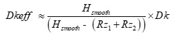
When copper foil with the same Rz roughness is bonded to each side of the core or prepeg, Dkeff is determined heuristically from published Dk by this simple correction factor [1]:
Equation 1.

where:
Hsmooth is the thickness of the dielectric as if the foil was removed
Dk = Dielectric constant published in laminate suppliers’ Dk/Df tables
Rz = 10-point mean equivalent to Rz(JIS) or Rz(DIN) published in foil suppliers’ data sheets. This is not to be confused with Rq, which is RMS value of roughness.
Rogers Corporation [4] understands this. That’s why they provide the “design” Dk in addition to their bulk Dk, as measured by TM650 clamped stripline resonator test method [7]. Design Dk is an average number using a differential phase length method from several different tested lots of material and on the most common thickness. This method is based on measuring phase difference from two identical microstrip transmission line geometries, of different lengths on the same panel. Because this is a real microstrip application, the dielectric is fully bonded to the copper and there is no air entrapment. Knowing the phase and length difference, the effective Dk is empirically determined.
The accuracy of the resultant effective Dk depends on several factors like:
-
-
fixture design
-
-
-
length ratio between two transmission lines
-
-
-
material thickness of the sample under test
-
-
-
the thickness of the copper
-
-
-
actual roughness of the foil on the microstrip circuit.
-
In lieu of actual Dk/Df tables, Rogers provides a handy impedance calculator as shown in in the RO4003C example of Figure 2. There are three Dk options available to use:
-
-
Z-axis bulk Dk
-
-
-
Dk values for specific frequencies
-
-
-
Dk values for characteristic impedance
-
The first radio button, as shown in Figure 2, gives the z-axis bulk Dk value of 3.55, as measured by TM650 2.5.5.5 test method manual. However, the value does not change when different frequencies are selected. This makes the number suspect since clearly design Dk does change over frequency. Thus this number can be considered equivalent to marketing data sheets, and should not be used.
When the middle radio button is selected, a Dk value for a specific frequency is displayed, which corresponds to a frequency entered in the lower right frequency box of Figure 2. This is the most useful option, since it allows the user to choose the right design Dk at whatever frequency they choose for their application, including characteristic impedance. This option already factors in the foil roughness effect, so no correction factor is needed to use in your simulator.
The last radio button selects a Dk for characteristic impedance calculation. It is a “design” Dk with yet a different Dk. Similar to the Bulk Dk option, it does not change over frequency. For any simulation tool other than the Rogers’s calculator, Bulk Dk and Dk values for characteristic impedance values should not be used.

Figure 2. Example of Rogers Corporation impedance calculator. For an 8-mil thick RO4003C dielectric, bulk Dk is 3.55 while design Dk over frequency is shown in bottom left window.
Under the information tab, the user can download design Dk over frequency, for a specified thickness, shown in the bottom left window of Figure 2. This data can be selected and copied to the clipboard and pasted into a spreadsheet for further processing.
Figure 3 plots design Dk vs. frequency for various thickness from 8 mils to 60 mils for RO4003C material. As can be seen, design Dk is not constant over frequency and furthermore it is different for different thicknesses, mainly due to the roughness of the foil that is already included in the measurement.
Thinner materials have a higher design Dk than thicker materials for the same roughness of foil. This is because when the foil teeth protrude into a thin dielectric material, there is a higher concentration of e-fields, resulting in higher capacitance between top and bottom copper layers. For thick dielectrics the foil teeth have less of an impact on capacitance and thus Dkeff, as described mathematically by Equation 1.
Since the roughness of the foil does not significantly influence the design Dk for thick laminates, we can assume the bulk Dk is roughly equivalent to design Dk over frequency for the 60-mil laminate.

Figure 3. Design Dk vs. frequency for various thickness of RO4003C from 8 mils to 60 mils mainly due to the roughness of the foil. Thinner material has a higher design Dk than thicker material, for the same roughness of foil.
Heuristically, we can rearrange Equation 1 and estimate the Rz roughness of the foil used on RO4003C laminate to be 6.302 μm from Equation 2.
Equation 2.

where:
Hsmooth is the thickness of the 8 mil (203 μm) laminate
DkBulk = 3.55 at 60 GHz for 60 mil (1524 μm) laminate
Dkeff = design Dk of 8 mil (203 μm) laminate at 60 GHz
A cross-section sample from a time domain reflectometry (TDR) demo board, courtesy of Picotest [6], was measured and is shown in Figure 4. The TDR demo board was fabricated with 8-mil thick Rogers RO4003C core laminate and cladded with 2 Oz copper foil.
Five highlighted random sample lengths of copper roughness, labeled Sample 1 to Sample 5 of Figure 4, were analyzed. The total length of each respective sample was then partitioned into five equal sections, similar to the blow-up picture of Sample 1, to measure the maximum peak to valley height of each section. The five measurements of each sample length were then averaged to determine the Rz roughness, as described under IPC TM650 2.2.17A [8] and shown in the table of Figure 4.
The mean value of Rz for the five samples was 6.176 μm with a standard deviation (SD) of 1.090 μm. This compares favorably with the estimated roughness of 6.302 μm, determined from Equation 2.

Figure 4. A cross-section sample from a Rogers RO4003C based TDR demo board, courtesy of Picotest [6], used to determine Rz roughness of the foil.
When we use the actual roughness measured from Figure 4 and Equation 1, we can then calculate Dkeff at 60 GHz for different thicknesses, shown in Table 1. As can be seen there is, less than 1% delta compared with design Dk reported from the calculator!
Table 1. Comparison of Roger’s Design Dk vs. Dkeff when simple correction factor applied to Bulk Dk at 60 GHz.
|
Height |
Height |
Bulk Dk |
Design Dk |
Rz |
Dkeff |
Delta |
|
8.0 |
203 |
3.550 |
3.785 |
6.176 |
3.780 |
-0.13% |
|
12.0 |
304 |
3.550 |
3.702 |
6.176 |
3.700 |
-0.04% |
|
16.0 |
406 |
3.550 |
3.657 |
6.176 |
3.661 |
0.12% |
|
20.0 |
508 |
3.550 |
3.625 |
6.176 |
3.638 |
0.37% |
|
32.0 |
812 |
3.550 |
3.580 |
6.176 |
3.605 |
0.69% |
|
60.0 |
1524 |
3.550 |
3.550 |
6.176 |
3.579 |
0.82% |
Rogers Corporation provides a handy calculator in lieu of Dk/Df tables in which “design” Dk values over frequency can be used directly without correcting for roughness. When an actual cross-section was analyzed, there was excellent correlation from corrected Dkeff using heuristic methods compared to design Dk from the calculator. Therefore, “design” Dk should be used for impedance modeling and PCB stackup design when using Rogers laminates.
References:
-
-
B. Simonovich, “A Tale of Two Data Sheets and What You Need to Know About Dielectric Constant (DK),” Signal Integrity Journal article, April 2022.
-
-
-
L. Simonovich, “A Practical Method to Model Effective Permittivity and Phase Delay Due to Conductor Surface Roughness,” DesignCon 2017, Santa Clara, USA.
-
-
-
Isola Group, 6565 West Frye, Chandler, AZ 85226.
-
-
-
Rogers Corporation, 2225 W. Chandler Blvd., Chandler, AZ 85224.
-
-
-
J. Coonrod, “Managing PCB Materials: Dielectric Constant (Dk)”, Rogers Corporation, Blog Article, Sep 11, 2018.
-
-
-
Picotest, Phoenix, AZ 85085.
-
-
-
IPC-TM-650, 2.2.17A, Test Methods Manual, “Surface Roughness and Profile of Metallic Foils (Contacting Stylus Technique).”
-
-
-
Bereskin, A. B. “Microwave Dielectric Property Measurements”, Microwave Journal, vol. 35, no.7, pp. 98 – 112.
-
A Tale of Two Data Sheets: Part1
Originally published SI Journal April 26, 2022
When doing printed circuit board (PCB) stackup and signal integrity (SI) impedance modeling, we need to get the dielectric material properties from the right sources. One important parameter for accurate impedance modeling is relative permittivity (εr) of the dielectric material, otherwise known as dielectric constant (Dk). The best source is from laminate suppliers’ data sheets. Though there is an issue with these I like to think of as, “a tale of two data sheets.”
Marketing data sheets, like the example shown in Figure 1 [6], are easily found on laminate suppliers’ websites. They are meant for quick comparison of dielectric properties to narrow your search for the right laminate for your application. Dielectric properties on marketing data sheets include mostly thermal and mechanical properties, which are important for the physical structure of the material and how it will perform with other material properties in the stackup during processing.
But marketing data sheets are not representative of what is needed to design an actual stackup, or to do impedance and SI loss modeling. Depending on glass style, resin content, thickness, Dk, and dissipation factor (Df) will be different for different cores and prepreg thicknesses for the same laminate. Marketing data sheets usually only report a typical Dk/Df at fifty percent resin content and two or three frequency points. Thickness is not specified. Furthermore, Dk and Df are not constant over frequency. So, using numbers from these data sheets will lead to inaccurate impedance and phase delay results.
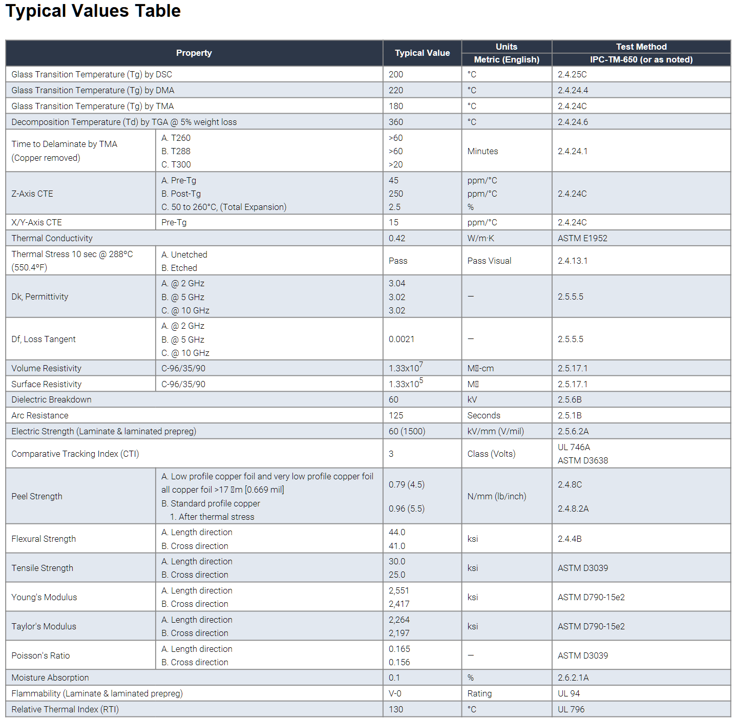
Figure 1. Example of a “Marketing” data sheet easily obtained from laminate supplier’s web site. Source Isola Group [6].
Instead, for transmission line modeling, one needs to use the same Dk/Df table data sheets PCB fabricators use to build the stackup. An example Dk/Df table is shown in Figure 2. Dk/Df tables provide the actual core and prepreg thicknesses, resin content, and Dk/Df for the different glass styles, over different frequencies. Depending on the stackup, a combination of thicknesses is often needed to meet impedance requirements. Each thickness will have a different Dk value.
In the example of Figure 2, Dk varies from 2.92 at 10 GHz for 1080 glass style to 3.19 at 10 GHz for 2116 glass style. This represents a Dk variation of -3.3% to 5.6% when compared to a Dk of 3.02 at 10 GHz specified in Figure 1.
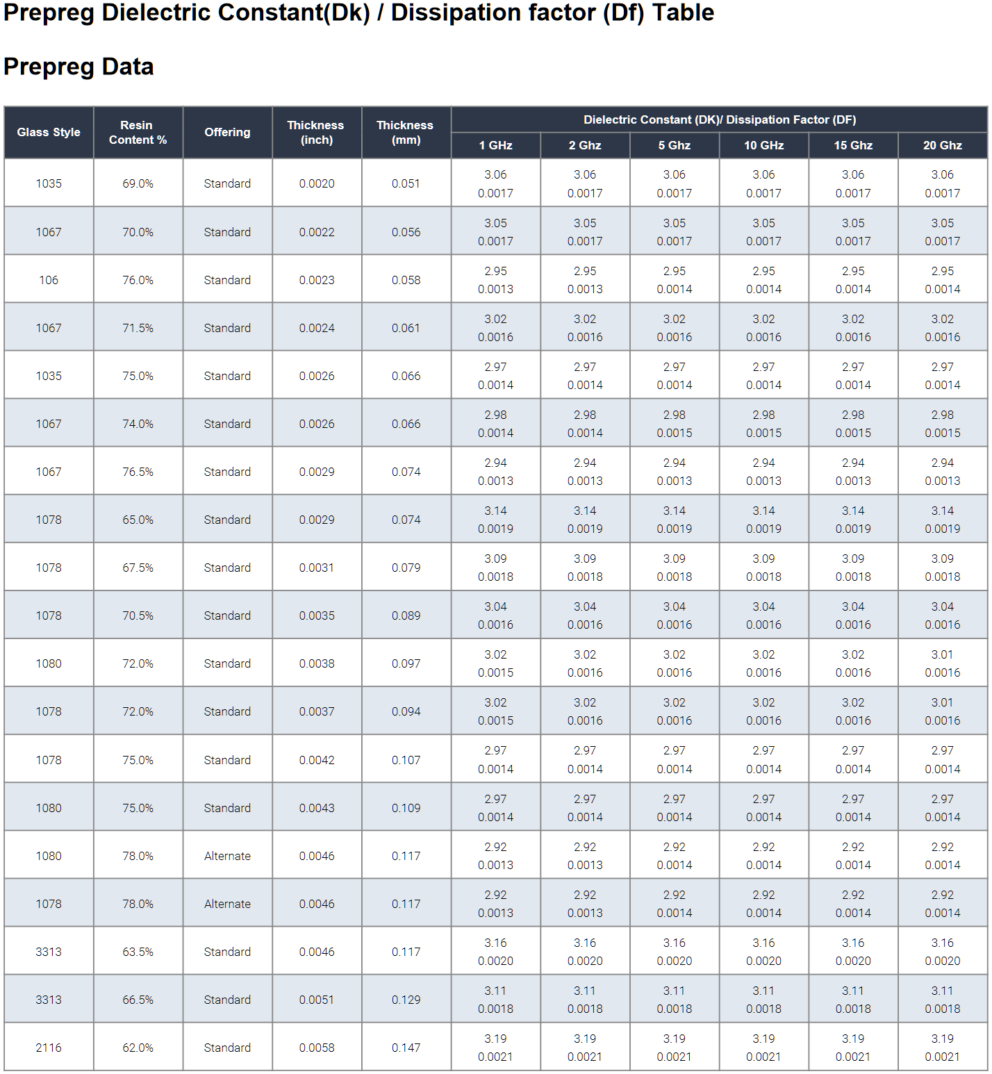
Figure 2. Example of a typical “Engineering” data sheet showing Dk/Df table for different glass styles and resin content over frequency. Source Isola Group [6].
Many engineers assume Dk published is the intrinsic property of the material. But, in fact, it is the effective Dk (Dkeff) measured by a specific industry standard test method. When they are compared against real measurements from a design application, there is often a discrepancy in Dkeff due to increased phase delay caused by surface roughness [1].
Dkeff is highly dependent on the test apparatus and conditions of how it is measured. One method commonly used by many laminate suppliers is the clamped stripline resonator test method, as described by IPC-TM-650 2.5.5.5, Rev C, Test Methods Manual [10].
Since all glass reinforced laminates are anisotropic, any stripline based test method, like TM-650 2.5.5.5, or Bereskin stripline test method [13], reports Dk values in which the E-fields are transverse to signal propagation. That is, if the signal propagation is in the x-y axis direction, then the Dk measured by this method is when E-fields are in the z-axis direction.
For Isola’s Dk/Df table [6], shown in Figure 2, Dk values were measured by TM-650 2.5.5.5 test method. From that data, the values for most of the constructions are calculated. Additional verification runs are performed to gather statistical data over time and validate that the calculations are reasonable and accurate.
The measurements are done under stripline conditions using a carefully designed resonant element pattern card. It is made with the same dielectric material to be tested. As shown in Figure 3, the card is sandwiched between two sheets of uncladded dielectric material under test. Then the whole structure is clamped between two large plates; each lined with copper foil and grounded. They act as reference planes for the stripline.
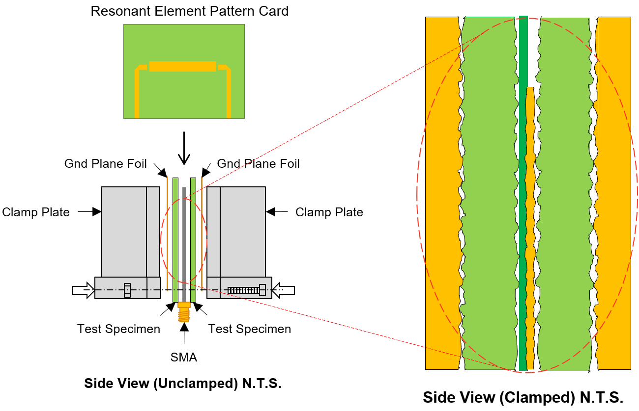
Figure 3. Illustration of clamped stripline resonator test method, as described by IPC-TM-650, 2.5.5.5, Rev C, Test Methods Manual [10].
This test method assures consistency of product when used in fabricated boards. It does not guarantee the values directly correspond to design applications.
Here is why:
Since the resonant element pattern card and material under test are not physically bonded together, air is entrapped between the various layers. These small air gaps are caused by the:
-
roughness of the copper foil plates in the fixture
-
roughness profile imprint left on the surface from the foil that was removed from the test samples
-
copper removed on the resonant element pattern card
Air entrapment, due to the TM-650 test method, is the primary reason for effective Dk and phase delay discrepancies between simulation using laminate suppliers’ Dk/Df tables and real measurements from a design application. The small air gaps result in a lower effective Dk than what would be measured in a real PCB because everything is pressed together with no air entrapment, as shown in a cross-section view of Figure 4.

Figure 4. Example of foil bonded to core or prepreg dielectric. Rz1 is rougher than Rz2 and Hsmooth is the thickness of the dielectric as if the foil was removed.
When copper roughness is different on each side of the dielectric, like the example shown in Figure 4, Dkeff is determined heuristically by this simple correction factor:
Equation 1.
where:
-
Hsmooth is dielectric core thickness from laminate suppliers’ Dk/Df table data sheet or pressed prepreg thickness from the PCB stackup drawing.
-
Rz1 and Rz2 are the conductor roughness of the foil for the respective side of the dielectric from foil suppliers’ data sheet. Typically, Rz is the 10-point mean roughness as measured by a mechanical profilometer.
-
Dk is dielectric constant from laminate supplier’s Dk/Df table data sheet.
In Figure 4, Rz1 is the roughness of the top foil, and Rz2 is the roughness of the bottom foil. In this example, Rz1 is rougher than Rz2. Hsmooth is the core thickness of the dielectric, as specified in the Dk/Df table, or pressed thickness of the prepreg, often shown on a stackup drawing. It is the thickness of the dielectric as if the foil was removed.
When copper foil with the same Rz roughness is bonded to each side of the core or prepeg, Dkeff can be simplified as:
Equation 2
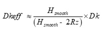
Figure 5 plots Dkeff over frequency derived from S21 phase or time delay (TD); Dkeff=(TDc0 ∕ length)2 from a Megtron-6 stripline case study [3]. This method is different than IPC-TM-650 test method in that it determines Dkeff from unwrapped phase delay rather than calculating Dk/Df from resonant peaks over the frequency range defined in the spec.
The blue plot is a simulated case based on core and prepreg Dk values from published Dk/Df tables at 12 GHz. When Dk is corrected due to roughness, using Equation 2, and resimulated, Dkeff is shown in pink. Although the Dkeff has improved, it still does not agree with the measured Dkeff from the device under test (DUT), shown in red.
Figure 5. Comparisons of simulated Dkeff over frequency vs. measured. The red plot is actual measured Dkeff from the DUT. The middle pink plot is a simulation using Dkeff corrected due to roughness. The bottom blue plot is simulated using Dk at 12 GHz as published in Dk/Df tables and non-causal roughness model. The green dashed plot is a simulation using Dkeff due to roughness; a causal Huray-Bracken roughness model was used. Modeled with Simbeor [11] and simulated with Keysight ADS [12].
The discrepancy between the pink and red plots is because Dkeff from Equation 2 only corrects the phase delay due to self capacitance (C11) per unit length of the transmission line. But roughness of the foil also increases the self inductance (L11) per unit length of the transmission line, which adds additional phase or time delay [4].
This is counter intuitive and can be confusing since we usually relate Dkeff to capacitance only. By definition, Dkeff is the ratio of the actual structure’s capacitance to the capacitance when the dielectric is replaced by air. But this is only true for static electric fields. For time-variant electromagnetic fields, Dkeff becomes frequency-dependent [14].
If the propagation delay (tpd) for a single transmission line, in seconds per unit length, is determined by:
Equation 3.
and c0 is the speed of light (~3.0E8 m/s) =1/sqrt(μ0 ε0 ); μ0 (4πE−7 H/m) and ε0 (8.8542E−12 F/m) is permeability and permittivity of free space respectively, then:
Equation 4.
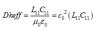
where: L11; C11 are self inductance in Henries per unit length and self capacitance in Farads per unit length respectively.
Equation 4 clearly shows that with an increase in self inductance there will be a proportional increase in Dkeff. This means for PCB transmission lines, calculating Dkeff=(TDc0 ∕ length)2 cannot be trusted to be the same as relative permittivity (εr) of the dielectric material. The consequence for doing so leads to inaccurate impedance predictions and non-causal time domain simulations, resulting in poor correlation to measurements.
A causal model, when simulated, does not produce any change in its output signal before there is a change in its input signal. When field solvers properly correct the self inductance, by applying the roughness correction factor to the imaginary portion of the complex impedance of the metal [4][5], the model is then causal. When combined with the corrected Dkeff for cores and prepregs from Equation 2, there is excellent correlation, as shown by the dashed green plot in Figure 5. Unfortunately, not all field solvers have causal roughness models to correct the inductance in the simulation.
Since there is no simple way to backtrack from a phase measurement to establish the right Dkeff to use for your modeling, especially for lossy stripline constructions, heuristic methods are an alternative.
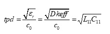
Using the right Dkeff for your modeling ensures a correct time domain reflectometer (TDR) impedance prediction, as shown in Figure 6. The red plot is measured differential TDR from [3]. When core and prepreg Dk from Dk/Df tables were used along with a non-causal roughness model in the simulation, the blue plot shows an overestimate for impedance. When Dkeff from Equation 2, and a non-causal roughness model was used in the simulation, the pink plot shows an underestimate in the impedance plot.
It is only when we apply a causal Huray-Bracken roughness model from [11], along with Dkeff from Equation 2, that we see the effect of the increased self inductance, shown by the green dashed line plot in Figure 6.
At first glance of Figure 6, one might interpret the pink plot as having better correlation to the measured red plot. But because the measured plot has an impedance ripple along its length, it is difficult to conclude which is the correct model from the TDR plots alone. It is only when we compare Dkeff derived from the green dashed phase delay plot from Figure 5 that we can conclude the green dashed line TDR plot is the correct impedance.
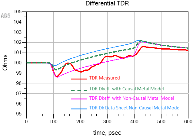
Figure 6. Simulated vs. measured differential TDR plots when different Dkeff was used in the model. The blue plot overestimates impedance when Dk from data sheets was used. The pink plot underestimates the impedance when Dkeff (Equation 2) and non-causal roughness model was used. The green dashed line plot is when Dkeff (Equation 2) and a causal Huray-Bracken roughness model were used. Modeled with Simbeor [11] and simulated with Keysight ADS [12].
Summary:
Dielectric constants from marketing data sheets cannot be trusted to properly design PCB stackups and model transmission lines for impedance and phase delay. Instead, laminate suppliers’ Dk/Df tables should be used.
Many laminate suppliers provide Dk/Df tables derived from a clamped stripline resonator test method [10] or similar Bereskin test method [13]. But the numbers do not factor the actual roughness of the foil. When a simple correction factor, based on the thickness of laminate and Rz foil roughness is considered, a more accurate value for Dkeff along with a causal roughness model can be used for impedance and transmission line modeling.
For PCB transmission lines, calculating Dkeff from phase or time delay measurement method cannot be trusted to be the relative permittivity of the dielectric material. Using this value will lead to inaccurate simulation results.
References:
1. L. Simonovich, “A Practical Method to Model Effective Permittivity and Phase Delay Due to Conductor Surface Roughness“, DesignCon 2017, Santa Clara, USA.
2. B. Simonovich, “Stackup Beware: Case Study of the Effects on Transmission Line Losses Due to Mixed Reference Plane Roughness”, Signal Integrity Journal article, August 10, 2021.
3. B. Simonovich, “PCB Fabrication: What SI/PI Engineers Need to Know for First Time Modeling Success”, DesignCon 2021 Spring Break Webinar Series, April 12-16, 2021.
4. V. Dmitriev-Zdorov, B. Simonovich, Igor Kochikov, “A Causal Conductor Roughness Model and its Effect on Transmission Line Characteristics“, DesignCon 2018, Santa Clara, USA.
5. J.E. Bracken, “A Causal Huray Model for Surface Roughness”, DesignCon 2012, Santa Clara, USA.
6. Isola Group, 6565 West Frye, Chandler, AZ 85226.
7. Circuit Foil, 6 Salzbaach, 9559 Wiltz, Grand Duchy of Luxembourg.
8. Rogers Corporation, 2225 W. Chandler Blvd., Chandler, AZ 85224.
9. J. Coonrod, “Managing PCB Materials: Dielectric Constant (Dk)”, Rogers Corporation, Blog Article, Sep 11, 2018
10. IPC-TM-650, 2.5.5.5, Rev C, Test Methods Manual
11. Simbeor THz [computer software].
12. Keysight ADS Keysight Advanced Design System (ADS) [computer software].
13. Bereskin, A. B. “Microwave Dielectric Property Measurements”, Microwave Journal, vol. 35, no.7, pp. 98 – 112
14. Wikipedia contributors. (2022, January 12). Relative permittivity. In Wikipedia, The Free Encyclopedia. Retrieved 18:14, January 14, 2022.
Characteristic Impedance – Where SI/PI Worlds Collide
Originally published Signal Integrity Journal, February 23, 2021
Signal and power integrity (SI/PI) simulations, measurements, and analysis usually live in two different worlds, but occasionally these worlds collide. One such collision occurs when we refer to characteristic impedance, Z0. Traditionally the PI world lives in the frequency domain while the SI world lives in the time domain.
When designing a power distribution network (PDN) in the PI world, we are mostly interested in engineering a flat impedance below a target impedance from DC to the highest frequency components of the transient current. Practically this is achieved with a network of capacitors with different values connected to the respective power planes as shown in Figure 1.

Figure 1 A simplified model of a typical PDN courtesy [1].
In the real world, there is no such thing as an ideal capacitor. There are always parasitic elements known as equivalent series inductance (ESL) and equivalent series resistance (ESR). Physical characteristics of the PCB, like component mounting inductance, plane spreading inductance, via and BGA ball inductance, along with voltage regulator module (VRM) characteristics also contribute to the impedance profile. When connected together, the interaction of capacitors and parasitic inductance and resistance create a transfer impedance profile with resonant peaks and anti-resonant nulls as shown in Figure 2.
The transfer impedance between the VRM and the load is calculated and plotted in the frequency domain with a log-log scale. The resulted impedance curve is then compared to the target impedance (Ztarget), which is estimated based on the allowed noise ripple and maximum transient current. The flat target impedance is frequency independent in the analysis.

Figure 2 Impedance profile of the PDN as viewed from the pads on the die power rail courtesy [1].
Resonant peaks are due to ESL of one capacitor connected in parallel with another capacitor. Anti-resonant nulls are due to the series combination of ESR, ESL, and C for each capacitor. Different capacitor values will have anti-resonant nulls at different frequencies.
But in the PI world, there is a rarely talked about characteristic impedance, Z0. In this case, it refers to the geometric average of the reactive impedance of a capacitor (XC) and reactive impedance of an inductor (XL).
Equation 1

At resonance, XL and XC intersect at the characteristic impedance and are equal as shown in Figure 3.

Figure 3 Inductive and capacitive reactance plot of ideal inductor and capacitor versus frequency. At resonance, XL and XC are equal and intersect at the characteristic impedance, Z0. Simulated with Pathwave ADS [6].
This is a very important observation, and it is where the SI/PI worlds collide.
In the SI world, characteristic impedance, Z0 refers to the instantaneous ratio of the voltage to current of a wave front traveling along a uniform transmission line without reflections. For an infinitely long uniform transmission line, Z0 equals the input impedance.
The characteristic impedance of a lossy transmission line is defined as:
Equation 2

Where R is resistance per unit length; G is conductance per unit length; L is inductance per unit length; and C is capacitance per unit length. For a lossless uniform transmission line, R and G are assumed to be zero and thus the characteristic impedance is reduced to:
Equation 3

Time Domain Reflectometer
In the SI world, we usually use a time domain reflectometer (TDR) to measure characteristic impedance, but more often than not, the measured impedance we get is not what we predicted with a 2D field solver. Many 2D field solvers used by most PCB FAB shops only calculate the lossless characteristic impedance of the cross-sectional geometry at a single frequency, defined by the dielectric constant (Dk). It has no input for conductor resistivity, dielectric loss, or how long the conductor(s) is.
So the issue is: we design the stackup, then do our SI modeling analysis based on stackup parameters and matching characteristic impedance. But the PCB FAB shop will often adjust the line width(s), over and above normal process variation, so that when measured, the impedance will fall within the specified tolerance, usually +/-10 percent.
Part of the problem lies with the method used to take the measurements. Most PCB FAB shops follow IPC-TM-650 Test Methods Manual [2]. But it has limitations because Z0 measured is derived and cannot be directly measured. The reason is the measurements include resistive and dielectric losses, up to the point where the measurement takes place along the TDR plot.
Resistive loss often results in a slow monotonic rise in the impedance profile, shown in the example TDR plot of Figure 4. IPC-TM-650 specifies a measurement zone between 30-70 percent to avoid probing induced ringing affecting the measurements. Most PCB FAB shops will measure an average impedance over this range, usually in the center region.
Depending on the linewidth, thickness and dielectric dissipation factor (Df), the slope of the monotonic rise will vary.

Figure 4 Example TDR plot showing slow monotonic rise in impedance due to resistive losses and IPC-TM-650 measurement zone.
The problem is that the IPC-TM-650 test method was last updated back in 2004, when higher dielectric loss, along with wider line widths and thicker copper weights, were used more often. A higher Df tends to compensate for resistive loss by flattening the slope as shown in Figure 5.
On the bottom left is a simulated TDR plot using a high loss dielectric with Df = 0.024. The right side has the exact same geometry properties except Df = 0.004. The average impedance, when measured at the 50 percent point, is 49.8 Ohms on the left side vs. 51.4 Ohms on the right side. We also confirm flatter slope for high loss material.
The actual characteristic impedance predicted by a Polar SI9000 2D field solver [5] in Figure 5 is 49 Ohms. For higher loss material, measuring within the measurement zone would pass without any issues. But for lower loss material, the resistive loss dominates and measuring within the measurement zone will give ~5 percent higher impedance reading compared to the higher loss material. The correct measurement point for Z0 is, in fact, the initial dip, equivalent to the field solver prediction. Depending on the tolerance specified, this may affect yield and cost.

Figure 5 Characteristic impedance prediction by Polar SI9000 2D field solver [5] (top). Simulated 2 inch TDR plots using a high loss dielectric (bottom left) vs. low loss dielectric with exactly the same geometry (bottm right). A higher Df compensates for higher resistive loss thereby flattening the curve. Simulated with Pathwave ADS [6].
Today, with the push to low loss dielectric and finer line widths with thinner copper weights, measuring the true transmission line characteristic impedance using a TDR becomes more challenging. This is even more so when measuring differential impedance, because a change in line width space geometry can have a more profound effect on measured differential impedance.
Using the first article build of a new design, as an example, let’s assume the correct characteristic impedance, when measured at the beginning of the slow monotonic rise of a TDR plot, is on the high end of nominal +10 percent tolerance. Let’s say it’s 54 Ohms. But because of the low loss dielectric and high resistive loss, the TDR measurement at the midpoint is now reading 5% higher at 57 Ohms. This would imply the impedance is now out of spec over nominal and the board would be scrapped.
The PCB fab shop will then go back and adjust the linewidth accordingly for the next build to bring the measurement within range to their measurement set up. Doing this effectively lowers the true nominal characteristic impedance!
If subsequent manufacturing variations pushes the measured impedance within the measurement zone on the low end of the -10 percent tolerance, say 44 Ohms, then the true characteristic impedance, if measured at the initial dip, will be 5 percent lower at 42 Ohms and be out of spec. But the board will pass because it was measured following IPC-TM-650 test method.
2-port Shunt Measurement
But what if there were another way? What if we could borrow impedance measuring techniques from the PI world to determine the true transmission line characteristic impedance in the SI world? Well there is. Enter the 2-port shunt measurement technique.
For example, in the PI world, to measure ESL and ESR of a chip capacitor, of a device under test (DUT), a 2-port shunt measurement is often used. It is much like the 4-point Kelvin measurement technique used to measure very low DC resistance.
The 2-port shunt measurement is usually done with a 2-port vector network analyzer (VNA). Port 1 of the VNA sends out a calibrated signal, and port 2 measures the voltage signal across the DUT. Often an isolation transformer is also used to break the inherent ground loop when measuring ultra-low impedances [3].
Once the measurements have been completed and S-parameters saved in touchstone format, further analysis can be done in your favorite SPICE simulator. Figure 6 is a generic schematic using popular Pathwave ADS [5] that can be used for 2-port shunt analysis.
When port 1 and port 2 are connected to port 1 of the DUT and port 2 of the DUT is grounded, the impedance of the DUT can be determined by [3];
Equation 4


Figure 6 Generic Pathwave ADS [6] schematic used for 2-port shunt analysis on a S2P file for DUT.
If we replace the DUT in Figure 6 with a capacitor and inductor, we get an impedance plot shown in Figure 7. As we saw earlier, when we take the geometric average of the inductive and capacitive reactance using Equation 1, we get the characteristic impedance. If we apply Equation 4 to the results of a 2-port shunt measurements of a capacitor and inductor, we get exactly the same results as shown in the top of Figure 7.
When we replace the capacitor and inductor with a S-parameter file of a transmission line model from Figure 5, we get the plot shown at the bottom of Figure 7. Except for the resonant nulls and peaks, up to a certain frequency, the impedance of a transmission line looks like the impedance of a capacitor when the far-end is open, and looks like the impedance of an inductor when the far-end is shorted. And because of that, this is where the two worlds collide!
If we take the geometric average of the impedance when the far-end is open (Zopen) or shorted (Zshort), we get the characteristic impedance at that frequency. We note where the red and blue impedance lines first intersect, is exactly the geometric average characteristic impedance at that frequency.
Also worth noting, the lines intersect at half of the frequency between the peaks and valleys at higher frequencies as well.

Figure 7 Impedance of inductive and capacitive reactance vs. frequency (top) and impedance of a transmission line vs. frequency (bottom) when the far-end is open (solid red) compared to when the far-end is shorted (solid blue). The intersection of the red and blue lines is exactly the characteristic impedance. Simulated with Pathwave ADS [5].
We can see this more clearly if we replot Figure 7 bottom using a linear scale for the x-axis, as shown in Figure 8. This is a very powerful observation. What this means is that when we measure the impedance half way between a peak and adjacent valley, of either the red or blue plot, it is the characteristic impedance of the transmission line at that frequency.
Thus, only an open or shorted end measurement is all that is needed to determine the characteristic impedance. For example, if we look at the red curve alone, then measure the first resonant null (m14) and adjacent peak (m15), the characteristic impedance (mag(Zopen) is measured exactly at one half the frequency between the two (m16).

Figure 8 Impedance of a transmission line vs. frequency on a linear scale when the far-end is open (solid red) compared to when the far-end is shorted (solid blue). The intersection of the red and blue lines half way between respective peaks and valleys is the characteristic impedance. Simulated with Pathwave ADS [6].
The first resonant red null and blue peak represent the quarter-wave resonant frequency due to open and shorted end. Each respective red null and blue peak following are the odd harmonics of the first quarter-wave resonant frequency.
Knowing this, we can now determine the phase or time delay (TD) of the transmission line as being one quarter of the period of the resonant frequency (f0).
Equation 5

Because resonant nulls and peaks occur at the resonant frequency, we can also determine the effective dielectric constant (Dkeff). Given the speed of light (c) = 11.8 in. per nanosecond, the length of the transmission line (len) in in. and quarter-wave resonant frequency (f0), Dkeff can be determined by:
Equation 6

CMP28 Case Study

Figure 9 Photo of a portion of CMP-28 test platform courtesy of Wildriver Technology [8] used for measurement validation.
To test the accuracy of this method, measured data from a CMP28 test platform, shown in Figure 9, was used for measurement validation. S-parameter (s2p) files from 2 inch and 8 inch single-ended stripline traces were provided as part of CMP-28 design kit courtesy of Wildriver Technologies [8]. The 6-inch transmission line segment S-parameter data was de-embedded courtesy of AtaiTec Corporation [9].
The characteristic impedance, based on trace geometry and stackup parameters, was modeled in Polar SI9000 [5]. Using Dk from data sheet tables @ 10GHz, and correcting for conductor roughness [10], the characteristic impedance predicted was 49.66 Ohms, as shown in Figure 10.

Figure 10 Polar SI9000 field-solver [5] characteristic impedance prediction of CMP28 trace geometry.
Touchstone S-parameter DUT files were connected with far-end open, shorted, and terminated as shown in Figure 11. The TDR plot, with far-end terminated, shows an impedance of 50.57 Ohms, when measured at the initial peak. Then it takes an immediate dip to approximately 50 Ohms before continuing with a slow monotonic rise with some ripples. If the DUT was a uniform trace, with connector discontinuity de-embedded, we would not see the initial peak followed by the dip. This signature strongly suggests that the DUT is not uniform and thus it is very difficult to determine the actual characteristic impedance using IPC-TM-650 test method alone.
But only after taking 2-port shunt measurements can we confirm the true characteristic impedance. As shown, Zoavg is 50.68 Ohms where the red and blue curves cross at 122.5 MHz, and confirms the true measurement point in the TDR plot is the initial peak. Both are about 1 Ohm higher compared with 2-D field solver results in Figure 10.
If the length of the transmission line simulated above is 6 in. and f0 =248.2 MHz, then TD = 1 ns and Dkeff = 3.92, using Equation 5 and Equation 6 respectively.

Figure 11 Measured results from a CMP28 test platform design kit, courtesy of Wildriver Technology [8].
But wait a minute. Why is Dkeff is higher than what was used in the 2-D field solver in Figure 10?
One reason is due to process variation of the material and fabrication. The actual Dkeff is determined by the final thickness of dielectric and the roughness of the copper, which also increases inductance affecting TD [10] [11]. But the main reason is Dk is frequency dependent and the value used in the field solver was at 10 GHz, based on laminate supplier’s Dk/Df tables.
Since TD, ultimately determines Dkeff, it does not represent the intrinsic property of the dielectric material. Because Dkeff varies with frequency, it was calculated at the first resonant null of 248.2 MHz, which is at a much lower frequency for Dk than the frequency originally used to select Dk in the field solver.
As can be seen in Figure 12, a simulated vs. measured 2-port shunt frequency plot, with far-end open and shorted, we get exactly the same information, compared to the traditional method used to validate characteristic impedance and Dkeff.
If we measure the 39th odd harmonic frequency (H) at 9.884GHz for the resonant null closest to 10GHz, equating to the value of Dk used in Polar Si9000 2D field solver, Dkeff can be calculated with Equation 7:
Equation 7

The bottom right plot of Figure 12, shows Dkeff simulated (blue) vs. measured (red). As we can see, the measured Dkeff at 248.7 MHz is 3.94; pretty much agreeing with our earlier calculation of 3.92 using Equation 6. Furthermore, when we compare Dkeff = 3.76 at 9.884 GHz, it agrees with our calculation for the 39th harmonic frequency from Equation 7. The reason there is still a slight difference in Dkeff is because the added delay due to inductance due to roughness [11] was not factored into the simulated model.
The bottom left is a TDR plot that shows measured impedance (red) vs. simulated (blue) over time. The marker at the beginning of the initial dip (m6) represents the characteristic impedance with highest frequency harmonics included in the incident step edge of TDR waveform. The marker at the end (m16) represents the impedance at twice the TD with high frequency harmonics attenuated due to dispersion of the lossy dielectric and resistance of trace length.
When we measure Zoavg_meas impedance of DUT at 9.884GHz, at the top plot of Figure 12, it agrees pretty well with the simulated and measured TDR plot at the initial step.

Figure 12 Comparison of PI world 2-port shunt measurement results for transmission line characteristic impedance and Dkeff compared to traditional SI world measurement results. Top plot is the 2-port shunt simulated vs. DUT impedance measurements at the fundamental and 39th harmonic frequencies. Bottom left is beginning and end impedance measurements on TDR plot. Bottom right measuring equivalent Dkeff at fundamental and 39th harmonic frequencies.
Summary and Conclusion
Sometimes, when SI and PI worlds collide, we get the best of both worlds. By borrowing a simple 2-port shunt impedance measuring technique from the PI world, we have another tool at our disposal to measure true characteristic impedance, TD, and effective Dk from a uniformly designed transmission line in the SI world. The advantage is, unlike a TDR measurement, measuring true characteristic impedance using 2-port shunt method is not influenced by resistive or dielectric losses.
References
-
L. Smith, S. Sandler, E. Bogatin, “Target Impedance Is Not Enough,” Signal Integrity Journal, Vol. 1, Issue 1, January 2019; URL: https://www.signalintegrityjournal.com/ext/resources/MEDIA-KIT-2019/January-2019-Print-Issue/SIJ-January-2019-Issue_eBook_-V2.pdf
-
IPC-TM-650 Test methods Manual, Number 2.5.5.7, “Characteristic Impedance of Lines on Printed Boards by TDR”, Rev. A, March, 2004
-
I. Novak, J. Millar, “Frequency-Domain Characterization of Power Distribution Networks,” Artech House, 685 Canton St., Norwood, MA, 02062, 2007.
-
Pathwave Advanced Design System (ADS) [computer software], Version 2021, URL: http://www.keysight.com/en/pc-1297113/advanced-design-system-ads?nid=-34346.0&cc=CA&lc=eng
-
Polar Instruments Si9000e [computer software], Version 2018, URL: https://www.polarinstruments.com/index.html
-
Keysight Pathwave Advanced Design System (ADS) [computer software], Version 2021, URL: http://www.keysight.com/en/pc-1297113/advanced-design-system-ads?cc=US&lc=eng.
-
E. Bogatin, “Bogatin’s Practical Guide to Transmission Line Design and Characterization for Signal Integrity”, Artech House, 685 Canton St., Norwood, MA, 02062, 2020
-
Wild River Technology LLC 8311 SW Charlotte Drive Beaverton, OR 97007. URL: https://wildrivertech.com/
-
AtaiTec Corporation, URL: http://ataitec.com/products/isd/
-
B. Simonovich, “A Practical Method to Model Effective Permittivity and Phase Delay Due to Conductor Surface Roughness“, DesignCon 2017 proceedings, Santa Clara CA.
-
V. Dmitriev-Zdorov, B. Simonovich, I. Kochikov, “A Causal Conductor Roughness Model and its Effect on Transmission Line Characteristics”, DesignCon 2018 proceedings, Santa Clara, CA.
-
I. Novak et al, “Determining PCB Trace Impedance by TDR: Challenges and Possible Solutions”, DesignCon 2013 proceedings, Santa Clara, CA.
-
S. Sandler, “Easy trick to measure plane impedance with VNA”, EDN Asia, 2014, URL: https://archive.ednasia.com/www.ednasia.com/STATIC/PDF/201410/EDNAOL_2014OCT21_TEST_TA_01.pdf%3FSOURCES=DOWNLOAD
Differential Impedance and Why We Care
Originally published in Signal Integrity Journal April 14,2020
What is Differential Impedance and Why do We Care?
Simply put, differential impedance is the instantaneous impedance of a pair of transmission lines when two complimentary signals are transmitted with opposite polarity. For a printed circuit board (PCB) this is a pair of traces, also known as a differential pair. We care about maintaining the same differential impedance for the same reason we care about maintaining the same instantaneous impedance of a single-ended (SE) transmission line: to avoid reflections.
There is really nothing special about differential pairs, other than maintaining the correct differential impedance. But you must understand the implications of the spacing between the traces in a pair.
The differential impedance is simply twice the odd-mode impedance of each trace. SE impedance is the impedance of a single trace and only equals the odd-mode impedance when there is little or no intra-pair coupling between them. When the traces are brought closer together, the differential impedance is reduced, unless the line widths are adjusted to compensate. (More about this later.)
Figure 1 shows the effect on intra-pair coupling of a pair of edge-coupled stripline traces driven differentially. The top figure shows electromagnetic fields surrounding a loosely coupled pair of traces 3.5 line-widths apart. The bottom figure shows a closely coupled pair at 1.5 line-widths apart. The red plus trace is current flowing into the page while the minus blue trace is current flowing out of the page.
The circular lines surrounding each trace are the magnetic fields representing loop inductance. The direction of rotation is based on current direction, using the right-hand rule. The electric field (e-field) lines are perpendicular to the magnetic field lines. They are a measure of capacitance.
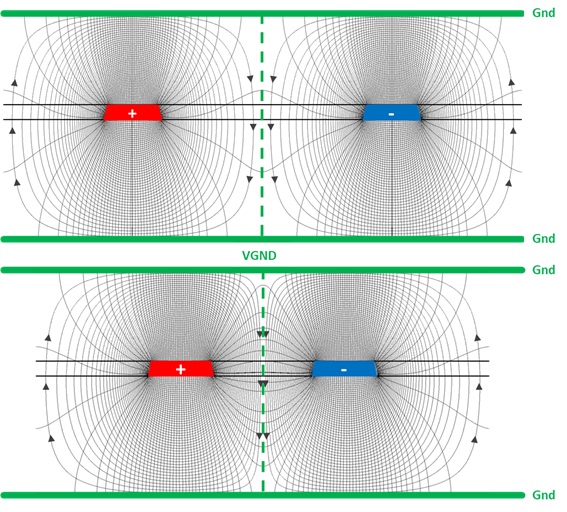
Figure 1. Effect on intra-pair coupling of a pair of edge-coupled stripline traces driven differentially. Top figure shows electromagnetic fields surrounding a loosely coupled pair of traces 3.5 line-widths apart. Bottom figure shows a closely coupled pair at 1.5 line-widths apart.
When the traces are loosely coupled, the electric and magnetic field lines are fairly symmetrical around each trace, and are mirror images of one another about the center line between them. Most of the respective e-field coupling is to the reference ground planes. As the traces are moved closer to one another, the counter-rotating rings compress about the centerline, lowering the inductance. At the same time, more of the e-field lines along the inside edge of each trace tend to couple to one another, increasing the capacitance.
Because of the way the EM-fields interact along the centerline, we can think of it as a virtual ground (VGND) reference plane. They behave exactly the same way as if there is a solid reference plane between them.
Odd-Mode Impedance
Consider a pair of equal width microstrip line traces, labeled 1 and 2, with a constant spacing between them as shown in Figure 2. Assuming lossless transmission lines, each individual trace, when driven in isolation, will have a SE characteristic impedance Zo, defined by the self-loop inductance (L11, L22) and self-capacitance (C11, C22) with respect to the GND reference plane.
When the pair of traces are driven differentially, the mode of propagation is odd. The electromagnetic field interaction is shown in Figure 1. When the intra-pair spacing is close, there will be electromagnetic coupling defined by the mutual inductance (Lm) and mutual capacitance (Cm).
The proximity of the traces to a reference plane influences the amount of electromagnetic coupling between traces. The closer the traces are to the reference plane, the lower the self-loop inductance and stronger self-capacitance; resulting in a lower mutual inductance, and weaker mutual capacitance between traces. The end result is a lower differential impedance.
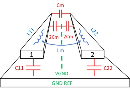
Figure 2. Pair of microstrip traces showing self-loop inductance (L11, L22), self-capacitance (C11, C22), mutual capacitance (Cm) and mutual inductance (Lm) when line 1 and line 2 are driven differentially.
A 2D field solver is usually used to extract the parameters for a given geometry. Once the resistance, inductance, conductance, and capacitance (RLGC) parameters are extracted, an L C matrix can be set up as follows:
L11 L12 C11 C12
L21 L22 C21 C22
The self-loop inductance and self-capacitance for trace 1 and 2 are L11, C11, L22, C22 respectively. In a perfectly symmetrical differential pair, the off-diagonal (12, 21) terms in each matrix are the mutual inductance and mutual capacitance respectively. The LC matrix can be used to determine the odd-mode impedance. It can be calculated by the following equation [1]:
Equation 1
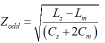
Where:
Zodd = odd mode impedance
Ls = self-loop inductance = L11 = L22
Cs = self-capacitance = C11 = C22
Lm = mutual inductance = L12 = L21
Cm = mutual capacitance = |C12 |=|C21|
Example
A Polar SI9000 field solver is used to compare a loosely coupled pair, with 4 mil traces, separated by 20 mil space, vs. a SE transmission line with the same dielectric thickness (see Figure 3). The LC matrix was extracted at 10GHz. As can be seen, the odd-mode impedance of the loosely coupled pair equals the characteristic impedance of the SE trace, and thus differential impedance would be the same.
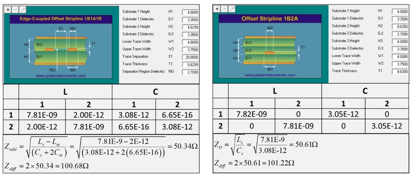
Figure 3. Comparison of a loosely coupled pair (left), with 4 mil traces, separated by 20 mil space, vs. a SE transmission line (right) with the same dielectric thickness. Odd-mode impedance of the loosely coupled pair equals the characteristic impedance of the SE trace.
But if you route a pair of traces with close coupling, the odd-mode impedance is less than the SE impedance for the same trace width (unless you adjust the line width). For example, on the left side of Figure 4, a 4-4-4 mil geometry has a differential impedance of 91 Ohms. In order to get 100 Ohms differential, the line width must be reduced to 3.35 mils and space adjusted to 4.65 mils to keep the same 12 mil center-center pitch, shown on right.

Figure 4. Comparison of 4-4-4 mil geometry (left) vs. 3.35-4.65-3.35 geometry (right) to achieve 100 Ohm differential impedance for the same center-center pitch.
But it doesn’t end there.
For some industry standards, there is usually a very short reach (VSR) spec which has a maximum channel loss defined. For example, the IEEE 802.3 CAUI-4 chip-module (C2M) spec budgets 7.5 dB at 12.89 GHz Nyquist frequency from the chip’s pins to a faceplate module’s pins, e.g. small form-factor pluggable (SFP) module. Because of modern top-of-rack routers and switches, it is not unusual to have 10 or more inches between the main switch chip and SFP module, the differential pair geometry design becomes important to satisfy both differential impedance and insertion loss (IL).
Reduced line width and tighter coupling results in higher loss over the length of the channel. Using the above examples, differential IL is plotted in Figure 5 for all three differential pairs. Loose coupling is shown in green; tight coupling without line width adjustment (Tight1) is shown in red, while tight coupling with line width adjustment (Tight2) is shown in blue.
As you can see, there is about a half dB difference at 12.89 GHz between loose coupling and both tight coupling examples over 10.6 inches. Tight coupling increases IL, regardless if line width is adjusted to meet differential impedance. In this example, there is only 0.1 dB delta between Tight1 and Tight2, which suggests most of the higher loss is due to tighter coupling.
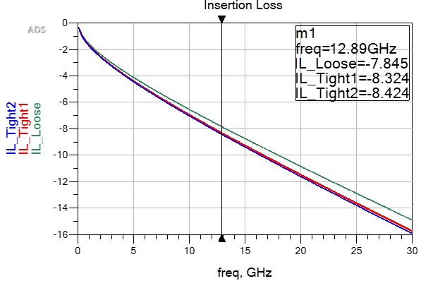
Figure 5. Differential IL comparison of loose coupling (green); Tight1 coupling without line width adjustments (red) and Tight2 coupling with line width adjustment (blue).
This can be explained by reviewing SE to differential mixed-mode conversion. Given a 4-port S-parameter, with SE port order as shown in Figure 6, the differential IL is determined by;
Equation 2
![]()
Where:
SDD21 = the differential IL defined by the ratio of the differential signaling coming out of port 2 to the differential signal going into port 1
S21 = the SE IL defined by the ratio of the SE signaling coming out of port 2 to the SE signal going into port 1
S43 = the SE IL defined by the ratio of the SE signaling coming out of port 4 to the SE signal going into port 3
S23 = far-end crosstalk coupling from port 3 to port 2
S41 = far-end crosstalk coupling from port 1 to port 4
As you can see from Equation 2, when the traces get closer together, and the coupling terms get larger, differential IL increases.
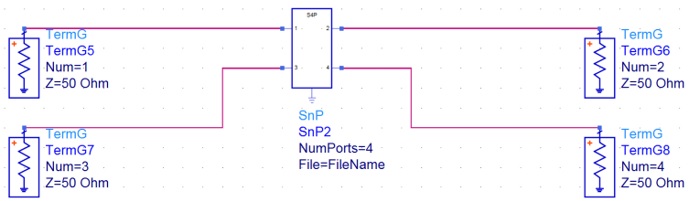
Figure 6. SE 4-port S-parameter port labeling.
Figure 7 plots differential TDR of all three examples. The steeper monotonic rise of the blue trace is due to higher resistive loss of 3.35 mil traces, as compared to the 4 mil traces in the other two examples.
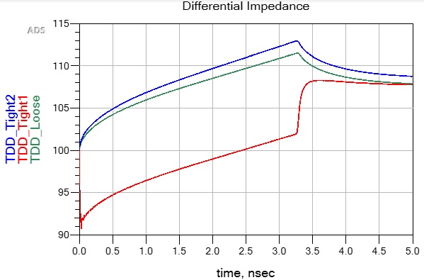
Figure 7. Differential TDR comparison of loose coupling (green); Tight1 coupling without line width adjustments (red) and Tight2 coupling with line width adjustment (blue).
To summarize then, it doesn’t matter if a differential pair is tightly coupled or loosely coupled. Properly engineered, both can be designed to properly match the output driver impedance. But as we have seen, each will have advantages and disadvantages.
Tighter coupling gives you better routing density at the expense of higher loss. Loose coupling allows for easier routing around obstacles and less loss. But in either case, they must be designed and measured for differential impedance.
So why is this important?
PCB fabrication shops use impedance as a metric to determine if the board has been fabricated to specification. Because the odd-mode impedance of a tightly spaced pair of traces depends on driving both traces differentially, you will not be able to determine the differential impedance by just measuring SE impedance of a tightly coupled pair like you could with two uncoupled traces.
References:
-
E. Bogatin, “Signal Integrity Simplified”, 3rd edition, Prentice Hall PTR, 2018
-
Keysight Advanced Design System (ADS) [computer software], (Version 2020)
-
Polar Instruments Si9000e [computer software] Version 2017
Simonovich-Cannonball Conductor Roughness Model Demystified
Recently on the SI-List there was great debate on whether or not my Cannonball model can be used to determine surface ratio and radius of sphere parameters needed for Huray roughness model from data sheets alone.
The author of this paper, “Conductor surface roughness modeling: From “snowballs” to “cannonballs”, [1] argues it is impossible to accurately model transmission lines from data sheets alone and seems to imply that because I had measured data in advance that I had magically “adjusted” Rz parameter to get such good correlation to measurements in my EDICon 2016 paper, “Practical Model of Conductor Surface Roughness Using Cubic Close-packing of Equal Spheres” [5].
Unfortunately his paper has created more confusion than clarity. To be clear, there is only ONE “Cannonball” model, and it is based on the cubic close packing of equal spheres, also known as face-centered cubic (FCC) packing.
The author of [1] also advocates using a material model identification methodology, similar to what I like to call the Design Feedback Method, shown in Figure 1. The author believes it is the only “accurate” way of determining printed circuit board (PCB) material properties for modeling.

Figure 1 Design Feed Back Method flow chart
This involves designing, building and measuring a test coupon with the intended PCB trace geometry to be used in final design. After modeling and tuning various parameters to best fit measured data, material parameters are extracted and then used in channel modeling software to design the final product.
The problem with this approach for many small companies is: TIME, RESOURCES, and MONEY.
-
Time to define stackup and test structures.
-
Time to actually design a test coupon.
-
Time to procure raw material – can take weeks, depending on scarcity of core/prepreg material.
-
Time to fabricate the bare PCB.
-
Time to assemble and measure.
-
Time to cross-section and measure parameters.
-
Time to model and fit parameters to measurements.
Then there is the issue of resources, which include having the right test equipment and trained personnel to get trusted measurements.
In the end this process ultimately costs more money, and material properties are only accurate for the sample from which they were extracted for the software and roughness model used. There is no guarantee extracted parameters reflect the true material properties.
There will be variation from sample to sample built from the same fab shop and more so from different fab shops because they have a different etch line and oxide alternative process.
For example Figure 2 shows measurements from two boards of the same design. As you can see there are differences in both insertion loss and TDR plots. Which curve do we use to fit parameters for material extraction to use in simulations? How many do we have to build and test to get a statistical sample of reality? How much time will this take? And how much money will it cost, especially if several PCB stackup geometries are required?

Figure 2 Comparison of insertion loss and TDR measurements of two boards of the same design
But, as Eric Bogatin often likes to say, “Sometimes an OK answer NOW is better than a good answer late”. For many signal integrity engineers, and design consultants, like myself, have to come up with an answer sooner, rather than later for many reasons. And depending on the issue at hand, those answers may be good enough. This was the initial motivation for my research.
So where do we get these parameters? Often the only sources are from manufacturers’ data sheets alone. But in most cases, the numbers do not translate directly into parameters needed for the EDA tools.
This paper will revisit the Cannonball model as it applies to the CMP-28 reference platform from Wildriver Technology [14], and as part of it I will show:
-
How to determine effective dielectric constant (Dkeff) due to roughness from data sheets alone.
-
How to apply my simple Cannonball stack model to determine roughness parameters needed for Huray model from data sheets alone.
-
How to apply these parameters using Simbeor software [10].
-
How to pull it all together with a simple case study.
But before we get into it, it is important to give a bit of background on material properties and PCB fabrication process.
Electro-deposited Copper
Electro-deposited (ED) copper is widely used in the PCB industry due to its low cost. A finished sheet of ED foil has a matte side and drum side. The matte side is usually treated with tiny nodules and is the side bonded to the core laminate. The drum side is always smoother than the matte side. For high frequency boards, sometimes the drum side of the foil is treated instead and bonded to the core. In this case it is known as reversed treated foil (RTF).
IPC-TM-650-2.2.17A defines the procedure for determining the roughness or profile of metallic foils used on PCBs. Profilometers are often used to quantify the roughness tooth profile of electro-deposited copper.
Nodule treated tooth profiles are typically reported in terms of 10-point mean roughness (Rz). Some manufacturers may also report root mean square (RMS) roughness (Rq). For standard foil this is the matte side. For RTF it is the drum side. Most often the untreated, or prepreg side, reports average roughness (Ra) in manufacturers’ data sheets.
With the realization of roughness having a detrimental effect on insertion loss (IL), copper suppliers began providing very low profile (VLP) and ultra-low profile (ULP) class of foils. VLP foils have treated roughness profiles less than 4 μm while ULP foils are less than 2 μm. Other names for ULP class are HVLP or eVLP, depending on the foil manufacturer.
It is important to obtain the actual vendor’s copper foil data sheet used by the respective laminate supplier for accurate modeling.
Oxide/Oxide Alternative Treatment
In order to promote good adhesion of copper to the prepreg material during the PCB lamination process, the copper surface is treated with chemicals to form a thin, nonconductive film of black or brown oxide. The controlled oxidation process increases the surface area, which provides a better bond between the prepreg and the copper surface. It also passivates the copper surface to protect it from contamination.
Although oxide treatment has been used for many years, eventually the industry learned that the lack of chemical resistance resulted in pink ring, which is indicative of poor adhesion between copper and prepreg. This weakness has led to oxide alternative (OA) treatments which rely on some sort of etching process, but no oxide layer is formed.
With the push for smoother copper to reduce conductor loss, newer chemical bond enhancement treatments, working at the molecular level, were developed to maintain copper smoothness, yet still provide good bonding to the prepreg.
Since OA treatment is applied to the drum side of the foil during the PCB Fabrication process, the OA roughness numbers should be used instead of Ra specified in foil manufacturer’s data sheets. RTF foil is modeled differently and discussed later in the case study.
Tale of Two Data Sheets
Everyone involved in the design and manufacture of PCBs knows the most important properties of the dielectric material are the dielectric constant (Dk) and dissipation factor (Df ).
Using Dk / Df numbers for stackup design and channel modeling from “Marketing” data sheets, like the example shown in Figure 3, will give inaccurate results. These data sheets are easily obtained when searching laminate supplier’s web sites.

Figure 3 Example of a “Marketing” data sheet easily obtained from laminate supplier’s web site. Source Isola Group.
Instead, real or “Engineering” data sheets, which are used by PCB fabricators to design stackups, should be used for PCB interconnect modeling. These data sheets define the actual thickness, resin content and glass style for different cores and prepregs. They include Dk / Df over a wide frequency range; usually from 100 MHz-10GHz.

Figure 4 Example of an “Engineering” data sheet showing Dk/Df for different glass styles and resin content over frequency. Source Isola Group.
Effective Dk Due to Roughness
Many engineers assume Dk published is the intrinsic property of the material. But in actual fact, it is the effective dielectric constant (Dkeff) generated by a specific test method. When simulations are compared against measurements, there is often a discrepancy in Dkeff, due to increased phase delay caused by surface roughness.
Dkeff is highly dependent on the test apparatus and conditions of how it is measured. One method commonly used by many laminate suppliers is the clamped stripline resonator test method, as described by IPC-TM-650, 2.5.5.5, Rev C, Test Methods Manual.
The measurements are done under stripline conditions using a carefully designed resonant element pattern card made with the same dielectric material to be tested. As shown in Figure 5, the card is sandwiched between two sheets of unclad dielectric material under test. Then the whole structure is clamped between two large plates; each lined with copper foil and are grounded. They act as reference planes for the stripline.

Figure 5 Illustration of clamped stripline resonator test method, as described by IPC-TM-650, 2.5.5.5, Rev C, Test Methods Manual
This method assures consistency of product when used in fabricated boards. It does not guarantee the values directly correspond to design applications.
This is a key point to keep in mind, and here is why.
Since the resonant element pattern card and material under test are not physically bonded together, there are small air gaps between the various layers that affect measured results. The small air gaps result in a lower Dkeff than what is measured in real applications using foil with different roughness bonded to the same core laminate. This is the primary reason for phase delay discrepancy between simulation and measurements.
If Dk and Rz roughness parameters from the manufacturers’ data sheets are known, then the effective Dk due to roughness (Dkeff_rough) of the fabricated core laminate can be estimated by [2]:
Equation 1

where: Hsmooth is the thickness of dielectric from data sheet; Rz is 10-point mean roughness from data sheet; Dk is dielectric constant from data sheet
Most EDA tools include a wideband causal dielectric model. To use it, you must enter Dk and Df at a particular frequency. I found it is usually best to use the values near the Nyquist frequency of the baud rate.
Modeling Copper Roughness
“All models are wrong but some are useful”– a famous quote by George E. P. Box, who was a British statistician in the mid-20th century. The same can be said when using various roughness models.
For example many roughness models require RMS roughness numbers, but often Rz is the only number available in data sheets, and vice versa. If Rz is defined as the sum of the average of the five highest peaks and the five lowest valleys of the roughness profile over a sample length, and Rq is the RMS value of that profile, then the roughness can be modeled as a triangular profile with a peak to valley height equal to Rz, as illustrated in Figure 6.

Figure 6 Triangular roughness profile model with peak to valley height equal to 10-point mean roughness Rz.
If we define the RMS height of the triangular roughness profile is equal to ∆, then:
Equation 2

And likewise, if we assume ∆ ~ Rq, then:
Equation 3
![]()
Several modeling methods were developed over the years to determine a roughness correction factor (KSR). When multiplicatively applied to the smooth conductor attenuation (αsmooth), the attenuation due to roughness (αrough) can be determined by:
Equation 4
![]()
Huray Model
In recent years, the Huray model has found its way into popular EDA software due to the continually increasing need for better modeling accuracy. The model is based on a non-uniform distribution of spherical shapes resembling “snowballs” and stacked together forming a pyramidal geometry.
By applying electromagnetic wave analysis, the superposition of the sphere losses can be used to determine the total loss of the structure. Since the losses are proportional to the surface area of the roughness profile, an accurate estimation of a roughness correction factor (KSRH) can be analytically solved by [4]:
Equation 5

Although it has been proven to be a pretty accurate model, it relied on analysis of scanning electron microscopy (SEM) pictures of the treated surface and tuning of parameters for best fit to measured data. This is not a practical solution if all you have is roughness parameters from manufacturers’ data sheets.
Simonovich “Cannonball” Conductor Roughness Model (A.K.A. Cannonball-Huray Model)
Building upon the work already done by Huray, and using the Cannonball stack principle, the sphere radius and flat base area parameters are easily estimated solely from roughness parameters published in manufacturers’ data sheets.
As illustrated in Figure 7 there are three rows of equal sized spheres stacked on a square tile base. Nine spheres are on the first row, four spheres in the middle row, and one sphere on top. This stacking arrangement is known as close-packing of equal spheres, but more commonly known as the “Cannonball” stack due to the method used by sailors to stack actual cannonballs aboard ships.

Figure 7 Cannonball-Huray physical model. The height of the stack is the RMS height of the peak to valley profile equal to Rz from data sheets.
If we could peer into the stack and imagine a pyramid lattice structure connecting to the center of all the spheres, then the total height is equal the height of two pyramids plus the diameter of one sphere.
Given the height of the Cannonball stack (∆) is equal to the RMS value of the peak to valley roughness profile; then from method described in my earlier papers, determining the sphere radius (r ), from Rz found in data sheets, can be further simplified and approximated as [13]:
![]()
and base area (Aflat) as:
Equation 7
![]()
Because the model assumes the ratio of Amatte/Aflat = 1, and there are only 14 spheres, the original Cannonball-Huray model can be further simplified to:
Equation 8

where: KCH (f) = Cannonball-Huray roughness correction factor, as a function of frequency; δ (f) = skin-depth, as a function of frequency in meters; r = the radius of spheres in meters (Equation 6)
CMP28 Case Study Revisited
To test the accuracy of the model, stackup details and measured data from a CMP28 test platform, design kit, courtesy of Wildriver Technology, shown in Figure 8, was used for model validation. The PCB stackup is shown in Figure 9
Two different sets of S-parameter (s2p) files from a 2 inch and 8 inch single-ended (SE) stripline traces shown were used in this study. The original set of measurements, from my previous papers, and a second set provided as part of CMP-28 design kit from another PCB were used for model correlation.
The 6 inch transmission line segment S-parameter data was de-embedded using Ataitec ISD software [8] for both sets of data.

Figure 8 Photo of a portion of CMP-28 test platform courtesy of Wildriver Technology used for model validation.

Figure 9 CMP-28 PCB Stackup
The PCB was fabricated with Isola FR408HR 3313 core and prepreg, with 1 oz. RTF. Dk and Df at 10GHz were obtained from the FR408HR data sheet found on their web site and shown in Figure 10 & Figure 11.

Figure 10 Isola FR408HR data sheet used for core dielectric properties.

Figure 11 Isola FR408HR data sheet used for prepreg dielectric properties.
The foil used on FR408HR core laminates is MLS, Grade 3, controlled elongation RTF from Oak-matsui. Roughness Rz parameters for drum and matte sides are 120μin (3.048 μm) and 225μin (5.715μm) respectively for 1 oz. copper foil.

Figure 12 MLS RTF foil data sheet used on FR408HR laminate.
An oxide or oxide alternative (OA) treatment is usually applied to the copper surfaces prior to final PCB lamination. When it is applied to the matte side of RTF, it tends to smoothen the macro-roughness slightly. At the same time, it creates a surface full of microvoids which follows the underlying rough profile and allows the resin to fill in the cavities, providing a good anchor.
MultiBond MP from Macdermid Enthone is an example of an oxide alternative micro-etch treatment commonly used in the industry. Typically 50 μin (1.27μm) of copper is removed when the treatment is completed, depending on the board shop’s process control, as per Figure 13.
In a subsequent paper by J.A. Marshall, presented at IPC APEX 2015 titled, “Measuring Copper Surface Roughness for High Speed Applications” [11], there is data supporting the hypothesis that RTF roughness gets smoother after OA application.

Figure 13 Macdermid Enthone MultiBond MP data sheet reference from their web site.
Table 1 summarizes the PCB design parameters, dielectric material properties and copper roughness parameters obtained from respective manufactures’ data sheets.
Table 1 CMP-28 Test Board and Data Sheet Parameters
| Parameter | FR408HR/RTF |
| Dk Core/Prepreg | 3.65/3.59 @10GHz |
| Df Core/Prepreg | 0.0094/0.0095 @ 10GHz |
| Rz Drum side | 3.048 μm |
| Rz Matte side before Micro-etch | 5.715 μm |
| Rz Matte side after Micro-etch | 4.445 μm |
| Trace Thickness, t | 1.25 mil (31.7μm ) |
| Trace Etch Factor | 60 deg |
| Trace Width, w | 11 mils (279.20 μm) |
| Core thickness, H1 | 12 mils (304.60 μm) |
| Prepreg thickness, H2 | 10.6 mils (269.00 μm) |
| GMS trace length | 6 in (15.23 cm) |
From Table 1 and by applying Equation 1, Dkeff of core and prepreg due to roughness were determined to be:

Next, the Cannonball model’s sphere radiuses, for matte and drum side of the foil, were determined to be:

Because most EDA tools only allow a single value for the radius parameter, the average radius (ravg) was determined to be:
Equation 9

Simbeor electromagnetic software from Simberian Inc. [10] was used for modeling the transmission lines. It includes the latest and greatest dielectric and conductor roughness models, including the Huray-Bracken causal metal model.
Solution explorer pane and solution tree, as shown in Figure 14, allows you to edit and view solution data as a tree structure. All parameters from Table 1 were entered here.
Simbeor requires two parameters; roughness factor (RF1) and sphere radius (SR1). Because the Cannonball model always has N=14 spheres and base area (Aflat) is always 36r2, r2 cancels out and RF1 can be simplified to:
Equation 10

Sphere radius (SR1) is ravg = 0.225 as calculated from Equation 9.

Figure 14 Simbeor Solution Explorer Pane and Solution Tree
The wideband causal dielectric model option was used to model dielectric properties over frequency. Effective Dk due to roughness for core and prepreg, calculated above, were substituted instead of data sheet values. Standard copper resistivity of 1.724e-8 ohm-meter was used.
After the transmission lines were modeled and simulated, the S-parameter results were saved in touchstone format. Keysight ADS [5] was used for further simulation analysis and comparison.
Dkeff can be derived from phase delay. This is also known as time delay (TD) and is often used as a metric for simulation correlation accuracy for phase. TD, as a function of frequency, in seconds, is calculated from the unwrapped measured transmission phase angle, and is given by:
Equation 11

and:
Dkeff , as a function of frequency, is then given by:
Equation 12

where:c = speed of light (m/s); Length = length of conductor (m)
Figure 15 compares the simulated results vs measurement of a 6inch, de-embedded stripline trace. The red plots are measured from CMP-28 design kit data. The data was bandwidth limited to 35 GHz. The blue plots are the original measured data used in my previous paper [5]. The green plots are modeled with data sheet values only with oxide alternative treatment applied. SE IL is shown on the left and Dkeff is shown on the right. As can be seen, there is excellent correlation.

Figure 15 Measured vs simulated insertion loss (left) and Dkeff (right) with OA etch treatment applied.
The author of [1] suggests is that because I had the measured data, Rz was “adjusted” to show excellent results. What he is implying is my “adjusting” the roughness, due to the oxide treatment, was the reason for such good results, in spite of the fact Macdermid’s OA data sheet reports typical 50 μin of copper removal after treatment and data from [11] showing RTF gets slightly smoother after OA treatment.
So ok, let’s see what happens if I didn’t adjust the roughness due to OA treatment. Instead of using Rz matte side after micro-etch (4.445 μm ) roughness, we will use 5.715 μm from data sheet.
This will affect Dkeff of prepreg and average sphere radius ravg , so we will recalculate them:

And average radius is:

Figure 16 compares the simulated results vs measurement. The red plots are measured from CMP-28 design kit data. The blue plots are the original measured data used in my previous paper [5]. The green plots are modeled with data sheet values only without oxide alternative treatment applied. SE IL is shown on the left and Dkeff is shown on the right.
As can be seen, there is still excellent correlation with insertion loss even though OA was not considered. As expected using the rougher number would increase effective Dk. But in the end the TDR plots in Figure 17shows impedance change is negligible.

Figure 16 Measured vs simulated insertion loss (left) and phase delay (right) without OA etch treatment applied.

Figure 17 Measured vs simulated TDR plots with OA etch treatment (left) and without (right).
Summary and Conclusions
By using Cannonball-Huray model, with copper foil roughness and dielectric material properties obtained solely from respective manufacturers’ data sheets, practical PCB interconnect modeling for high-speed design is now achievable using commercial field-solving software employing Huray model.
Measured results from two different boards confirmed there are variations due to manufacturing that would affect material model extraction method accuracy.
When oxide alternative treatment was not considered, even though the matte side roughness of RTF gets smoothened during the PCB fabrication process, the simulated results still show excellent correlation to the original measured data from previous paper [5].
References
[1] Y. Slepnev, “Conductor surface roughness modeling: From “snowballs” to “cannonballs”.
[2] B. Simonovich, “A Practical Method to Model Effective Permittivity and Phase Delay Due to Conductor Surface Roughness”. DesignCon 2017, Proceedings, Santa Clara, CA, 2017
[3] L. Simonovich, “Practical method for modeling conductor roughness using cubic close-packing of equal spheres,” 2016 IEEE International Symposium on Electromagnetic Compatibility (EMC), Ottawa, ON, 2016, pp. 917-920. doi: 10.1109/ISEMC.2016.7571773.
[4] Huray, P. G. (2009) “The Foundations of Signal Integrity”, John Wiley & Sons, Inc., Hoboken, NJ, USA., 2009
[5] L.Simonovich, “Practical Model of Conductor Surface Roughness Using Cubic Close-packing of Equal Spheres”, EDICon 2016, Boston, MA
[6] Keysight Advanced Design System (ADS) [computer software], (Version 2017). URL: http://www.keysight.com/en/pc-1297113/advanced-design-system-ads?cc=US&lc=eng.
[7] Isola Group S.a.r.l., 3100 West Ray Road, Suite 301, Chandler, AZ 85226. URL: http://www.isola-group.com/
[8] Ataitec, URL: http://ataitec.com/products/isd/
[9] V. Dmitriev-Zdorov, B. Simonovich, I. Kochikov, “A Causal Conductor Roughness Model and its Effect on Transmission Line Characteristics”, DesignCon 2018 Proceedings, Santa Clara, CA, 2018
[10] Simberian Inc., 2629 Townsgate Rd., Suite 235, Westlake Village, CA 91361, USA, URL: http://www.simberian.com/
[11] John A. Marshall, “Measuring Copper Surface Roughness for High Speed Applications”, IPC APEX Expo 2015.
[12] Macdermid Enthone, Multibond MP, Inner Layer Oxide Alternative Bonding. URL: https://electronics.macdermidenthone.com/products-and-applications/printed-circuit-board/surface-treatments/innerlayer-bonding
[13] B. Simonovich, “PCB Interconnect Modeling Demystified”. DesignCon 2019, Proceedings, Santa Clara, CA, 2019.
[14] Wild River Technology LLC 8311 SW Charlotte Drive Beaverton, OR 97007. URL: https://wildrivertech.com/
Perils of Crossing Split Planes
 I recently came across this YouTube video spoof of Chuck Norris doing the spits across two aircraft wings above the clouds and it occurred to me that it was a perfect metaphor for what happens when a digital signal, propagating along a microstrip trace, crosses a split plane on a printed circuit board (PCB). If Chuck Norris and his merry band of paratroopers standing on his head were the signal, then at the split of two reference planes, we would see an impedance mismatch which manifests itself as a positive peak in the time domain reflection (TDR) plot for the duration of the discontinuity.
When discussing signal integrity (SI) issues there is always a great debate when signals on one layer of PCB crossing over split or a slot in the reference planes. On the one hand, some argue that this should never be done because of the increased risk in crosstalk and possible failure to pass electromagnetic compatibility (EMC) compliance. On the other hand, others stressed that if the width of the gap and power/ground layers in the stackup were engineered carefully, this may not be as big of an issue. So who’s right?
Well, like all things involving signal integrity, the answer is, “it depends”. And the best way to answer “it depends” is to put in the numbers.
When I decided to investigate this, I thought to myself I would just set up a couple of simple simulations to explore the issues. Of course, once you get into it, you find other scenarios to check out, then another, and before long you have amassed a lot of data. So I decided to capture it all in a white paper.
Here is a brief summary of the results.
To see just how much of an issue this is I set up a topology using Keysight ADS as shown in Figure 1. Two transmission line segments before and after the gap section (TL17, TL18) were modeled with internal 2D field solver. The gap section (SNP139) was modeled and simulated with Momentum 3D planar field solver in order to properly capture the electromagnetic effects as the signals cross the gaps. The S-parameter results were saved as touchstone format and brought back into the ADS schematic.
A 50 mil gap was chosen for worst case and a 5 mil gap was chosen for best case. As expected, when the topology was driven differentially from Port 1, the 50 mil gap results, shown in red, had a higher impedance discontinuity compared to the 5 mil gap, shown in blue.

Figure1 Keysight ADS general schematic (top) used to model and simulate a microstrip crossing a split plane. Red and blue plots (bottom) are differential impedance comparison of 50 mil vs 5 mil gaps respectively.
Figure 2 shows simulated results of incident/transmitted signals; near-end/far-end crosstalk (NEXT/FEXT) when the gap between the split planes was reduced from 50 mils (blue plots) down to 5 mils, and the thickness of dielectric from layer2 to layer 3 was reduced from 45 mils to 2 mils (red plots). Compared to the scenario with no gap (black plots) there was no appreciable increase in crosstalk.

Figure 2 Comparison of SE Incident/Transmitted voltage, NEXT/FEXT for 50 mil gap (blue) and thick dielectric under the gap vs 5 mil gap and thin dielectric under the gap (red). As expected the closer proximity of reference plane under the gap results in less incident reflection and NEXT while minimizing risetime degradation in transmitted signal and FEXT.
From a signal integrity perspective, one may conclude that crossing a split plane may be ok, with certain caveats. But in terms of passing EMC, there is still risk and doubt. For instance we see that there is still some current flow along each side of the split when we reduce the thickness between Layer 2 and 3. The combination of the split plane and diverted return current along the split creates an efficient slot antenna which will radiate noise.
Since a real design may have many interdependencies affecting the final performance, it is difficult to come up with a general rule that says if you do this, and minimize that you will be ok; and because of that, I’m still on the side of staying away from crossing split planes. When you can’t, then a more detailed analysis should be done based on the actual layout and stackup of the board; or look for other alternatives that can mitigate noise radiation; like adding extra external shielding for instance.
In the end it is what I always like to say about engineering, “it’s what you don’t know you don’t know that can ruin your day”. In today’s high-speed designs we can no longer restrict our thinking in terms of signal integrity, power integrity or EMC alone. We must consider all three and become educated or at least aware of the other disciplines. Had we only been concerned about signal integrity, without being aware of EMC we would have probably made the wrong conclusion, and in the end the final product might well have failed EMC compliance tests.
For more detail you can down load the white paper I wrote titled, “Split Planes and What Happens When Microstrip Signals Cross Them” from my web site here.
Practical Modeling of High-speed Channels
As Dave Dunham from Molex Corp. likes to say, “When designing high-speed serial links beyond 10 GB/s, everything matters”. In order to ensure first time success at these speeds, accurate channel modeling is a prerequisite. This is especially true for long backplane channels.
 Although many EDA tools include the latest and greatest models for conductor surface roughness and wide-band dielectric properties, obtaining the right parameters to feed the models is always a challenge. Often the only sources are from data sheets alone. But in most cases, the numbers do not translate directly into parameters needed for the EDA tools. So how do we get these parameters?
One way is to follow the design feedback method which involves designing, building and measuring a test coupon, then extracting the parameters through tuning simulation to measurement. Although this method is pretty practical and accurate, a significant amount of expertise and equipment is required to design, build and measure the test coupon, which takes significant amount of time and money.
But, as Eric Bogatin often likes to say, “Sometimes an OK answer NOW! is better than a good answer late.” As a high-speed signal integrity practitioner and backplane architect, I often have to come up with an answer sooner, rather than later because of the impact to time and cost to my clients. And that’s why I have been motivated over the last few years to research and develop simple methodologies to accurately determine parameters to feed into modern EDA tools.
If you went to this year`s EDICon 2017 in Boston, and attended the High-speed Digital Symposium session, you would have heard me speak on a “Practical Modeling of High-speed Channels Based on Data Sheet Input”, which was the title of my presentation.
For those of you who could not attend, I have made available an annotated slide deck. You can download a copy from my web site.
What you will learn:
-
How to use my Cannonball model to determine Huray roughness parameters from data sheet alone
-
How to determine effective dielectric constant due to roughness from data sheets alone
-
How to apply these parameters in the latest version of Polar Si9000e Field Solver
-
How to pull it all together using Keysight ADS software
And this is an example of simulation results compared to measurements you can expect to see:

