Archive for the ‘Useful Equations’ Category
COUPLED TRANSMISSION LINES AND CROSSTALK
Originally published Signal Integrity Journal August 9, 2022
When two coplanar parallel traces running in close proximity over the coupled length, as shown in Figure 1, they are electromagnetically coupled together.
When two complementary signals are transmitted, there is mutual electromagnetic coupling defined by the amount of mutual inductance and capacitance. This is known as differential signaling. The differential impedance (Zdiff), is the instantaneous impedance of a pair of transmission lines.
The impedance of each trace, when driven differentially, is known as the odd-mode impedance (Zodd). Conversely, when each trace is driven with the same polarity, the impedance of each trace is known as the even-mode impedance (Zev).
Differential impedance is simply twice the odd-mode impedance:
Equation 1
![]()
When Zodd = Zev, the traces are deemed to be uncoupled and there will be no crosstalk (XTalk). The characteristic impedance (Zo) of a single trace, in isolation, is equal to the geometric average (Zavg) of Zodd and Zev. When Zodd and Zev are not equal, there will be some level of XTalk, depending on the space between traces. In this case, Zo is approximately equal to Zav and is given as;
Equation 2
![]()
Crosstalk
There are two types of XTalk generated; Near-End (NEXT), or backwards XTalk, and Far-End (FEXT), or forward XTalk.

Figure 1 Illustration of NEXT and FEXT. As the aggressor signal propagates from port 3 to port 4, Near-End XTalk appears on port 1 and Far-End XTalk appears on port 2 after one time delay (TD) of the interconnect.
NEXT
Refer to Figure 1. Through electromagnetic coupling, NEXT voltage (Vb) is related to the coupled current through a terminating resistor (not shown) at port 1; when driven by an aggressor voltage (Va) at port 3. When port 1 is terminated, the backward crosstalk coefficient (Kb) is defined by;
Equation 3

where;
Vb = the voltage at port 1
Va = the peak voltage of the aggressor at port 3
The general signature of the NEXT waveform, for a gaussian step aggressor, is shown in Figure 2. Va is the aggressor voltage at port 3 of Figure 1. Vb is the NEXT voltage at port 1. The NEXT voltage continues to increase in response to the rising edge of the aggressor until it saturates after the aggressor’s rise-time. The green waveform (VaFE) is the aggressor voltage at port 4 after one time delay (TD). The duration of Vb waveform lasts for 2TD of the coupled length.

Figure 2 NEXT voltage signature, Vb in response to a gaussian step aggressor, Va. The duration of NEXT is equal to 2TD of the coupled length. VaFE is the aggressor voltage shown after one TD. simulated with Teledyne Lecroy WavePulser 40iX software.
When TD is equal to one-half of the linear risetime, the NEXT voltage becomes saturated. The minimum length to reach saturation is known as the saturated length (Lsat), and is given by [1]:
Equation 4

where:
Lsat = the saturation length for near-end cross talk in inches
RT = Linear risetime to reach Va in ns
c = the speed of light = 11.8 in nsec
Dkeff = The effective dielectric constant surrounding the trace.
For example, a signal with a linear RT of 0.1nsec, to reach an aggressor voltage of 1V using FR4 material, with a Dkeff of 4, the saturation length in stripline is;

Important note: In PCB stripline construction, Dkeff is the Dk of the dielectric mixture of core and prepreg. But in microstrip, without solder mask, Dkeff is the mixture of Dk of air and Dk of the substrate. It is very difficult to predict the exact Dkeff in microstrip without a field solver, but a good approximation can be obtained by [3];
Equation 5

where;
DkeffMS = effective dielectric constant surrounding the trace in microstrip
Dk = Dielectric constant of the material
H = Height of dielectric
W = trace width
t = trace thickness
For example, a signal with a linear RT of 0.1ns, to reach an aggressor voltage of 1V and DkeffMS of 2.64, the saturation length in microstrip is;
If the coupled length (Lcoupled) is less than Lsat, the NEXT voltage will peak at a value less than the saturated NEXT voltage. The actual NEXT voltage, Vb is scaled by the ratio of coupled length to saturation length and is given by [1]:
Equation 6

For example, for a coupled of length of 100 mils and saturated length of 295 mils, NEXT voltage will be (100/295) or 33.9% of the saturated NEXT voltage.
NEXT vs Coupled Length in Stripline
Figure 3 plots NEXT voltage vs coupled lengths for 100mils, 295 mils and 590 mils representing less than, equal to and greater than Lsat respectively. For a coupled stripline geometry modeled with Polar SI9000 field solver (Figure 3B), Kb is 0.065.
Each length was then simulated in Polar Si9000 and touchstone files were imported into Keysight PathWave ADS software for further analysis. The results are plotted in Figure 3A.

Figure 3 Example of NEXT voltage vs couple lengths of 100 mils, 295 mils and 590 mils in stripline, with linear rise time of 0.1ns. Modeled with Polar Si9000 and simulated with Keysight PathWave ADS.
As can be seen, using a 1V aggressor with a linear risetime of 0.1ns and a saturated length of 295 mils, the NEXT voltage is 63.2 mV, compared to full saturated NEXT voltage of 64.8 mV. With a coupled length of 100 mils, NEXT voltage saturates at 22.2 mV, for the duration of the aggressor’s risetime, compared to 22.03mV predicted by Equation 6 [1].
NEXT vs Coupled Length in Microstrip
Similarly, Figure 4 plots NEXT voltage vs coupled lengths for 100mils, 363 mils and 590 mils for Lsat respectively. For a coupled microstrip geometry modeled with Polar SI9000 field solver (Figure 3B), Kb is 0.055.
Each length was then simulated in Polar Si9000 and touchstone files were imported into Keysight PathWave ADS software for further analysis. The results are plotted in Figure 4A.

Figure 4 Example of NEXT voltage vs couple lengths of 100 mils, 363 mils and 590 mils in microstrip with linear rise time of 0.1ns. Modeled with Polar Si9000 and simulated with Keysight PathWave ADS.
As can be seen, using a 1V aggressor with a linear risetime of 0.1ns and a saturated length of 363 mils, the NEXT voltage is 54.6 mV, compared to full saturated NEXT voltage of 54.9 mV. With a coupled length of 100 mils, NEXT voltage saturates at 15.8 mV for the duration of the aggressor’s risetime, compared to 15.1mV predicted by Equation 6.
The magnitude of the NEXT voltage is a function of the coupled spacing between the two traces. As the two traces are brought closer together, the mutual capacitance and inductance increases and thus the NEXT voltage, Vb, will increase as defined by [1];
Equation 7

where;
Vb = NEXT voltage on victim
Kb = Backward crosstalk (NEXT) coefficient
Va = Aggressor voltage
Cm = Mutual capacitance per unit length
Lm = Mutual inductance per unit length
Co = Trace capacitance per unit length
Lo = Trace inductance per unit length
Unfortunately, the only practical way to calculate Kb is to use a 2D field solver to get the inductive and capacitance matrix elements from a field solver.
Alternatively, if only the odd and even mode impedances are known, then Kb is given as [2];
Equation 8

where;
Zterm = Victim input termination impedance, normally the characteristic impedance (Zo) of a single trace.
When Zterm is open circuit, Kb’ is given as [2];
Equation 9

FEXT:
FEXT voltage is correlated to the coupled current through a terminating resistor (not shown) at port 2 of Figure 1. The forward crosstalk coefficient, Kf, is equal to the ratio of FEXT voltage to aggressor voltage at the far end, defined as;
Equation 10

where;
Vf = the far end crosstalk voltage
VaFE = the peak voltage of the aggressor at far-end
The general signature of the FEXT waveform, for a gaussian step aggressor, is shown in Figure 5. Vf is the forward crosstalk voltage at port 2 of Figure 1. VaFE is the aggressor voltage appearing at the far end port 4. FEXT voltage differs from NEXT in that it only appears as a pulse at TD after the signal is launched. In this example, the negative going FEXT pulse is the derivative of the aggressor’s rising edge at TD. The opposite is true on the falling edge of an aggressor.

Figure 5 FEXT voltage signature, Vf, is forward crosstalk (FEXT) voltage in response to a gaussian step aggressor voltage, VaFE. Simulated with Teledyne Lecroy WavePulser 40iX software.
Unlike the NEXT voltage, the peak value of FEXT voltage scales with the coupled length. It peaks when its amplitude grows to a level comparable to the voltage at 50% of the aggressor’s risetime at TD as shown in Figure 6. In this example, the coupled lengths are: 2, 4, 6, 8 and 10 inches respectively.
As the wave propagates along the transmission line, the RT degrades due to the dielectric dispersive loss. In the same way the aggressor waveform couples FEXT voltage onto the victim, FEXT voltage also couples noise back onto the aggressor affecting the risetime as shown. Due to superposition, the aggressor waveform shown at each TD is the sum of the FEXT voltage and the original transmitted waveform that would have appeared at TD with no coupling.

Figure 6 Microstrip FEXT voltage increase vs TD for coupled lengths of 2, 4, 6, 8 and 10 inches respectively. Simulated with Teledyne Lecroy WavePulser 40iX software.
If the rise-time at TD is known, the FEXT voltage, Vf can be predicted by [1];
Equation 11

where;
Vf = FEXT voltage on victim
VaFE = Far-end aggressor voltage
Kf = FEXT coefficient
Cm = Mutual capacitance per unit length
Lm = Mutual inductance per unit length
Co = Trace capacitance per unit
Lo = Trace inductance per unit length
RT = Risetime of aggressor signal at TD in sec
c = Speed of light
Dkeff = Effective dielectric constant surrounding the trace
Len = Length of trace
Although the inductive and capacitive matrix elements can be obtained using a 2D field solver, the rise-time is more difficult to predict because of risetime degradation, as well as impedance variations along the line causing reflections. But worst of all, as seen in Figure 6, is the forward crosstalk coupling affecting the aggressor’s risetime makes it next to impossible to predict.
The only practical way to calculate Kf is to model and simulate the topology using a circuit simulator that supports coupled transmission lines. The circuit simulator should have an integrated 2D field solver built in to allow automatic generation of a coupled transmission line model from the cross-sectional information.
Since the dielectric surrounding the traces in stripline is more homogeneous, than it is in microstrip, the best way to significantly reduce, or eliminate FEXT, is to route the traces in stripline geometry. Depending on the difference in Dk between core and prepreg used in the stackup, there is always a probability there will be some small amount of FEXT generated. The best way to mitigate this is to choose cores and prepregs to have similar values of Dk when designing the stackup.
References:
[1] E. Bogatin, “Signal Integrity Simplified”, 2nd edition, Prentice Hall PTR, 2010
[2] B. Young, “Digital Signal Integrity”, Upper Saddle River, NJ: Prentice Hall, 2001
[3] E. O. Hammerstad, “Equations for Microstrip Circuit Design,” 1975 5th European Microwave Conference, 1975, pp. 268-272, doi: 10.1109/EUMA.1975.332206.
[4] E. Bogatin, B. Simonovich, “Dramatic Noise Reduction using Guard Traces with Optimized Shorting Vias”, DesignCon 2013, Santa Clara, CA, USA
Single-ended to Mixed-Mode Conversions
Originally published in Signal Integrity Journal Magazine, July 2020
Signal Integrity (SI) engineers almost always have to work with S-parameters. If you haven’t had to work with them yet, then chances are you will sometime in your SI career. As speed moves up in the double-digit GB/s regime, many industry standards are moving to serial link-based architectures and are using frequency domain compliance limits based on S-parameter measurements.
A vector network analyzer (VNA) is the test instrument of choice to measure S-parameters from a device under test (DUT). By definition, each S-parameter (Sij) is the ratio of the sine wave voltage coming out of a port to the sine wave voltage that was going in to a port (Equation 1). Each S-parameter is complex with a magnitude and a phase.

Suffice it to say, for mathematical reasons, the indexes refer to the port in which the voltages are coming or going. This is counter intuitive to our normal train of thought and is important to be cognisant of this relationship when working with S-parameters.
Single-ended S-parameters
Figure 1 shows an example of a 1-Port, 2-Port and 4-Port DUTs and their respective S-parameter matrices representing uniform transmission lines with respective port index labelling. Each S-parameter in the matrix are single-ended measurements from one port to another.
A 1-Port DUT has one S-parameter (S11) shown in red. It is the ratio of the voltage coming out of Port 1 to the voltage going into Port 1. As a measure of reflected energy out of Port 1, it is also known as return loss (RL)
A 2-Port DUT has 4 S-parameters shown in blue. S-parameters with the same index subscript numbers, i.e. S11, S22 are RL. S-parameters with alternate index subscript numbers, are a measure of transmitted energy and is the ratio of the voltage coming out of a Port to the voltage going into the opposite Port. It is also known as insertion loss (IL). For example, S12 is the ratio of the voltage coming out of Port 1 to the voltage going into Port 2, whereas S21 is the ratio of the voltage coming out of Port 2 to the voltage going into Port 1.

Figure 1 From left to right examples of 1-Port (Red), 2-Port (Blue), 4-Port (Black) DUTs and their respective S-parameter matrices.
A 4-Port DUT has 16 S-parameters, divided into 4 quadrants, shown in black. As you can see the number of S-parameter combinations is the square of the number of ports. In this example, the top left quadrant 1 and bottom right quadrant 4 are the same as individual 2-Port DUTs with different port indices. They are described as:
Quadrant 1:
-
S11 is the ratio of the voltage coming out of Port 1 to the voltage going into Port 1. It is the RL out of Port 1.
-
S12 is the IL and is the ratio of the voltage coming out of Port 1 to the voltage going into Port 2. It is the IL from Port 2 to Port 1.
-
S21 is the ratio of the voltage coming out of Port 2 to the voltage going into Port 1. It is the IL from Port 1 to Port 2. For a uniform transmission line, S21 = S12.
-
S22 is the ratio of the voltage coming out of Port 2 to the voltage going into Port 2. It is the RL out of Port 2. For a uniform transmission line, S22 = S11.
Quadrant 4:
-
S33 is the ratio of the voltage coming out of Port 3 to the voltage going into Port 3. It is the RL out of Port 3
-
S34 is the ratio of the voltage coming out of Port 3 to the voltage going into Port 4. It is the IL from Port 4 to Port 3
-
S43 is the ratio of the voltage coming out of Port 4 to the voltage going into Port 3. It is the IL from Port 3 to Port 4. For a uniform transmission line, S43 = S34.
-
S44 is the ratio of the voltage coming out of Port 4 to the voltage going into Port 4. It is the RL out of Port 4. For a uniform transmission line, S44 = S33
S-parameters in the top right quadrant 2 and bottom left quadrant 3 describe the near-end and far-end coupling of the respective ports. When unwanted coupling happens at the near-end, it is referred to as near-end cross talk, or NEXT. When it happens at the far-end, it is known as far-end crosstalk, or FEXT.
Quadrant 2:
-
S13 is the ratio of the voltage coming out of Port 1 to the voltage going into Port 3. It is the coupling or NEXT from Port 3 to Port 1.
-
S14 is the ratio of the voltage coming out of Port 1 to the voltage going into Port 4. It is coupling or FEXT from Port 4 to Port 1.
-
S23 is the ratio of the voltage coming out of Port 2 to the voltage going into Port 3. It is coupling or FEXT from Port 3 to Port 2.
-
S24 is the ratio of the voltage coming out of Port 2 to the voltage going into Port 4. It is coupling or NEXT from Port 4 to Port 2.
Quadrant 3:
-
S31 is the ratio of the voltage coming out of Port 3 to the voltage going into Port 1. It is the coupling or NEXT from Port 1 to Port 3.
-
S32 is the ratio of the voltage coming out of Port 3 to the voltage going into Port 2. It is coupling or FEXT from Port 2 to Port 3.
-
S41 is the ratio of the voltage coming out of Port 4 to the voltage going into Port 1. It is coupling or FEXT from Port 1 to Port 4.
-
S42 is the ratio of the voltage coming out of Port 4 to the voltage going into Port 2. It is coupling or NEXT from Port 2 to Port 4.
Although there is no industry standard for labeling a 4 or more port DUT, a practical way is to use the port order shown so that the 2-Port DUT is a subset of the top left quadrant of the 4-Port DUT. When you do this, the port order labeling is consistent as you increase the number of ports; with odd ports on the left and even ports on the right. S12 and S21 always describe the IL terms; while S13 and S31 define the NEXT terms.
But sometimes 3rd party 4-port S-parameters are labeled with ports 1 and 2 are on the left side, while ports 3 and 4 are on the right side. In this configuration, S31 and S42 are now the IL terms. This is counter intuitive when moving from 2-Port to 4 or more Port DUT and leading to potential confusion when cascading S-parameters to build a channel model, or converting to mixed-mode S-parameters. Whenever you get S-parameter files from 3rd party, it is always prudent to test it and compare IL plots against port order to ensure you are using them correctly.
Typically, 4-port S-parameters are saved in Touchstone format with a .snp extension, where n is the number of ports. Many Electronic Design Automation (EDA) and circuit simulation software tools allows you to view and plot S-parameters from Touchstone files.
Figure 2 is a schematic of a 4-port S-parameter component used in Keysight ADS. When the component is linked to appropriate .s4p touchstone file and ports connected as shown, the 16-port S-parameter matrix can be plotted and analyzed.

Figure 2 Keysight ADS schematic used to plot 4-Port single-ended S-parameters.
The 1-port and 2-port S-parameters are included in the same plot as the 4-port S-parameters plotted in Figure 3. The top left (red) and bottom right (green) quadrants plot the return loss (RL) and insertion loss (IL), while the top right (blue) and bottom left (magenta) quadrants plot the NEXT and FEXT.

Figure 3 An example of 4-Port S-parameter single-ended plots of a uniform transmission line.
Mixed-mode S-parameters
SI engineers often have to check channel models and S-parameter measurements against industry standard compliance plots. Many of those plots are in terms of mixed-mode S-parameters, which means the single-ended measurements need to be converted to mixed-mode matrix.
Two single-ended transmission lines with coupling are also known as a differential pair, as shown in Figure 4. When we talk about single-ended transmission lines with coupling, we are usually interested in their single-ended properties like characteristic impedance (Zo), phase delay, and NEXT/FEXT relationships as described above.
But when we talk about a differential pair, we are interested in the mixed-mode S-parameters like differential and common signals and how they interact within the pair. Because we are describing the exact same interconnect, they are equivalent.
When describing a differential pair, there are only four possible outcomes in response to an input signal as defined by the mixed-mode S-parameter matrix:
-
A differential signal enters the differential pair and a differential signal comes out
-
A differential signal enters the differential pair and a common signal comes out
-
A common signal enters the differential pair and a differential signal comes out
-
A common signal enters the differential pair and a common signal comes out

Figure 4 Single-ended vs mixed-mode S-parameter matrices of two coupled transmission lines.
Mixed-mode S-parameters in each quadrant are described as:
SDD Quadrant (Red):
-
SDD11 is the ratio of the differential signal coming out of Port 1 to the differential signal going into Port 1. It is the differential RL out of Port 1.
-
SDD12 is the ratio of the differential signal coming out of Port 1 to the differential signal going into Port 2. It is the differential IL from Port 2 to Port 1.
-
SDD21 is the ratio of the differential signal coming out of Port 2 to the differential signal going into Port 1. It is the differential IL from Port 1 to Port 2.
-
SDD22 is the ratio of the differential signal coming out of Port 2 to the differential signal going into Port 2. It is the differential RL out of Port 2.
SDC Quadrant (Blue):
-
SDC11 is the ratio of the differential signal coming out of Port 1 to the common signal going into Port 1.
-
SDC12 is the ratio of the differential signal coming out of Port 1 to the common signal going into Port 2.
-
SDC21 is the ratio of the differential signal coming out of Port 2 to the common signal going into Port 1.
-
SDC22 is the ratio of the differential signal coming out of Port 2 to the common signal going into Port 2.
SCD Quadrant (Magenta):
-
SCD11 is the ratio of the common signal coming out of Port 1 to the differential signal going into Port 1.
-
SCD12 is the ratio of the common signal coming out of Port 1 to the differential signal going into Port 2.
-
SCD21 is the ratio of the common signal coming out of Port 2 to the differential signal going into Port 1.
-
SCD22 is the ratio of the common signal coming out of Port 2 to the differential signal going into Port 2.
SCC Quadrant (Green):
-
SCC11 is the ratio of the common signal coming out of Port 1 to the common signal going into Port 1.
-
SCC12 is the ratio of the common signal coming out of Port 1 to the common signal going into Port 2.
-
SCC21 is the ratio of the common signal coming out of Port 2 to the common signal going into Port 1.
-
SCC22 is the ratio of the common signal coming out of Port 2 to the common signal going into Port 2.
Single-ended S-parameters, with port order shown in Figure 4, can be mathematically converted into mixed-mode S-parameters using equations shown in Table 1.

Alternatively, Keysight ADS can simplify this process using equations on 4-Port single-ended or using 4-port Balun components, as shown in Figure 5.

Figure 5 Keysight ADS schematic used to convert from 4-Port single-ended to 2-Port mixed-mode S-parameters using equations or 4-Port Balun components. Differential and common port numbering as D1, D2, C1, C2 respectively.
Figure 6 plots mixed-mode S-parameters from equations in Table 1. Each quadrant is color coded to coincide with the respective table quadrants.

Figure 6 An example of 4-Port S-parameter mixed-mode plots of a differential transmission line.
References:
[1] M. Resso, E. Bogatin, “Signal Integrity Characterization Techniques”, International Engineering Consortium, 300 West Adams Street, Suite 1210, Chicago, Illinois 60606-5114, USA, ISBN: 978-1-931695-93-0
https://www.amazon.com/Signal-Integrity-Characterization-Techniques-Bogatin-ebook/dp/B07P9277WY/ref=sr_1_fkmr0_1?keywords=bogaitn+resso&qid=1581289220&sr=8-1-fkmr0
[2] A. Huynh, M. Karlsson, S. Gong (2010). Mixed-Mode S-Parameters and Conversion Techniques, Advanced Microwave Circuits and Systems, Vitaliy Zhurbenko (Ed.), ISBN: 978-953-307-087-2,InTech, Available from: http://www.intechopen.com/books/advanced-microwave-circuits-and-systems/mixed-mode-s-parameters-and-conversion-techniques.
[3] Alfred P. Neves, Mike Resso, and Chun-Ting Wang Lee, “S-parameters: Signal Integrity Analysis in the Blink of an Eye”, Signal Integrity Journal, https://www.signalintegrityjournal.com/articles/432-s-parameters-signal-integrity-analysis-in-the-blink-of-an-eye
Keysight Advanced Design System (ADS) [computer software], (Version 2020). URL: http://www.keysight.com/en/pc-1297113/advanced-design-system-ads?cc=US&lc=eng.
Differential Impedance and Why We Care
Originally published in Signal Integrity Journal April 14,2020
What is Differential Impedance and Why do We Care?
Simply put, differential impedance is the instantaneous impedance of a pair of transmission lines when two complimentary signals are transmitted with opposite polarity. For a printed circuit board (PCB) this is a pair of traces, also known as a differential pair. We care about maintaining the same differential impedance for the same reason we care about maintaining the same instantaneous impedance of a single-ended (SE) transmission line: to avoid reflections.
There is really nothing special about differential pairs, other than maintaining the correct differential impedance. But you must understand the implications of the spacing between the traces in a pair.
The differential impedance is simply twice the odd-mode impedance of each trace. SE impedance is the impedance of a single trace and only equals the odd-mode impedance when there is little or no intra-pair coupling between them. When the traces are brought closer together, the differential impedance is reduced, unless the line widths are adjusted to compensate. (More about this later.)
Figure 1 shows the effect on intra-pair coupling of a pair of edge-coupled stripline traces driven differentially. The top figure shows electromagnetic fields surrounding a loosely coupled pair of traces 3.5 line-widths apart. The bottom figure shows a closely coupled pair at 1.5 line-widths apart. The red plus trace is current flowing into the page while the minus blue trace is current flowing out of the page.
The circular lines surrounding each trace are the magnetic fields representing loop inductance. The direction of rotation is based on current direction, using the right-hand rule. The electric field (e-field) lines are perpendicular to the magnetic field lines. They are a measure of capacitance.
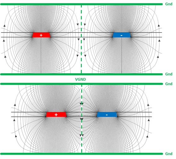
Figure 1. Effect on intra-pair coupling of a pair of edge-coupled stripline traces driven differentially. Top figure shows electromagnetic fields surrounding a loosely coupled pair of traces 3.5 line-widths apart. Bottom figure shows a closely coupled pair at 1.5 line-widths apart.
When the traces are loosely coupled, the electric and magnetic field lines are fairly symmetrical around each trace, and are mirror images of one another about the center line between them. Most of the respective e-field coupling is to the reference ground planes. As the traces are moved closer to one another, the counter-rotating rings compress about the centerline, lowering the inductance. At the same time, more of the e-field lines along the inside edge of each trace tend to couple to one another, increasing the capacitance.
Because of the way the EM-fields interact along the centerline, we can think of it as a virtual ground (VGND) reference plane. They behave exactly the same way as if there is a solid reference plane between them.
Odd-Mode Impedance
Consider a pair of equal width microstrip line traces, labeled 1 and 2, with a constant spacing between them as shown in Figure 2. Assuming lossless transmission lines, each individual trace, when driven in isolation, will have a SE characteristic impedance Zo, defined by the self-loop inductance (L11, L22) and self-capacitance (C11, C22) with respect to the GND reference plane.
When the pair of traces are driven differentially, the mode of propagation is odd. The electromagnetic field interaction is shown in Figure 1. When the intra-pair spacing is close, there will be electromagnetic coupling defined by the mutual inductance (Lm) and mutual capacitance (Cm).
The proximity of the traces to a reference plane influences the amount of electromagnetic coupling between traces. The closer the traces are to the reference plane, the lower the self-loop inductance and stronger self-capacitance; resulting in a lower mutual inductance, and weaker mutual capacitance between traces. The end result is a lower differential impedance.
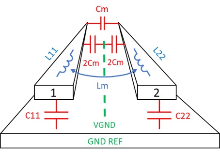
Figure 2. Pair of microstrip traces showing self-loop inductance (L11, L22), self-capacitance (C11, C22), mutual capacitance (Cm) and mutual inductance (Lm) when line 1 and line 2 are driven differentially.
A 2D field solver is usually used to extract the parameters for a given geometry. Once the resistance, inductance, conductance, and capacitance (RLGC) parameters are extracted, an L C matrix can be set up as follows:
L11 L12 C11 C12
L21 L22 C21 C22
The self-loop inductance and self-capacitance for trace 1 and 2 are L11, C11, L22, C22 respectively. In a perfectly symmetrical differential pair, the off-diagonal (12, 21) terms in each matrix are the mutual inductance and mutual capacitance respectively. The LC matrix can be used to determine the odd-mode impedance. It can be calculated by the following equation [1]:
Equation 1
Where:
Zodd = odd mode impedance
Ls = self-loop inductance = L11 = L22
Cs = self-capacitance = C11 = C22
Lm = mutual inductance = L12 = L21
Cm = mutual capacitance = |C12 |=|C21|
Example
A Polar SI9000 field solver is used to compare a loosely coupled pair, with 4 mil traces, separated by 20 mil space, vs. a SE transmission line with the same dielectric thickness (see Figure 3). The LC matrix was extracted at 10GHz. As can be seen, the odd-mode impedance of the loosely coupled pair equals the characteristic impedance of the SE trace, and thus differential impedance would be the same.
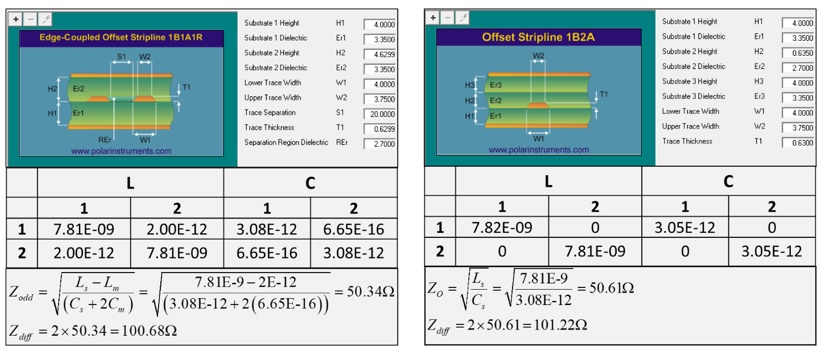
Figure 3. Comparison of a loosely coupled pair (left), with 4 mil traces, separated by 20 mil space, vs. a SE transmission line (right) with the same dielectric thickness. Odd-mode impedance of the loosely coupled pair equals the characteristic impedance of the SE trace.
But if you route a pair of traces with close coupling, the odd-mode impedance is less than the SE impedance for the same trace width (unless you adjust the line width). For example, on the left side of Figure 4, a 4-4-4 mil geometry has a differential impedance of 91 Ohms. In order to get 100 Ohms differential, the line width must be reduced to 3.35 mils and space adjusted to 4.65 mils to keep the same 12 mil center-center pitch, shown on right.

Figure 4. Comparison of 4-4-4 mil geometry (left) vs. 3.35-4.65-3.35 geometry (right) to achieve 100 Ohm differential impedance for the same center-center pitch.
But it doesn’t end there.
For some industry standards, there is usually a very short reach (VSR) spec which has a maximum channel loss defined. For example, the IEEE 802.3 CAUI-4 chip-module (C2M) spec budgets 7.5 dB at 12.89 GHz Nyquist frequency from the chip’s pins to a faceplate module’s pins, e.g. small form-factor pluggable (SFP) module. Because of modern top-of-rack routers and switches, it is not unusual to have 10 or more inches between the main switch chip and SFP module, the differential pair geometry design becomes important to satisfy both differential impedance and insertion loss (IL).
Reduced line width and tighter coupling results in higher loss over the length of the channel. Using the above examples, differential IL is plotted in Figure 5 for all three differential pairs. Loose coupling is shown in green; tight coupling without line width adjustment (Tight1) is shown in red, while tight coupling with line width adjustment (Tight2) is shown in blue.
As you can see, there is about a half dB difference at 12.89 GHz between loose coupling and both tight coupling examples over 10.6 inches. Tight coupling increases IL, regardless if line width is adjusted to meet differential impedance. In this example, there is only 0.1 dB delta between Tight1 and Tight2, which suggests most of the higher loss is due to tighter coupling.
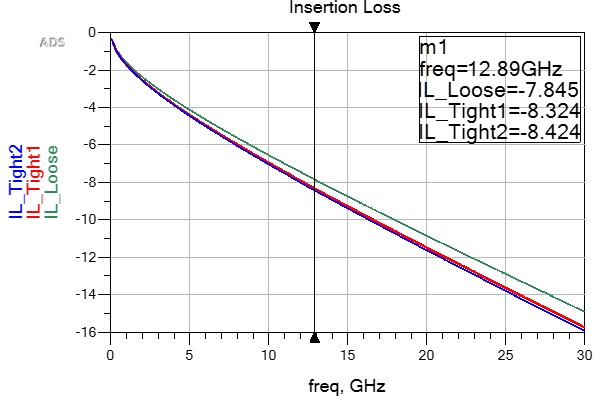
Figure 5. Differential IL comparison of loose coupling (green); Tight1 coupling without line width adjustments (red) and Tight2 coupling with line width adjustment (blue).
This can be explained by reviewing SE to differential mixed-mode conversion. Given a 4-port S-parameter, with SE port order as shown in Figure 6, the differential IL is determined by;
Equation 2
![]()
Where:
SDD21 = the differential IL defined by the ratio of the differential signaling coming out of port 2 to the differential signal going into port 1
S21 = the SE IL defined by the ratio of the SE signaling coming out of port 2 to the SE signal going into port 1
S43 = the SE IL defined by the ratio of the SE signaling coming out of port 4 to the SE signal going into port 3
S23 = far-end crosstalk coupling from port 3 to port 2
S41 = far-end crosstalk coupling from port 1 to port 4
As you can see from Equation 2, when the traces get closer together, and the coupling terms get larger, differential IL increases.
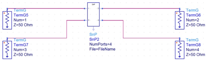
Figure 6. SE 4-port S-parameter port labeling.
Figure 7 plots differential TDR of all three examples. The steeper monotonic rise of the blue trace is due to higher resistive loss of 3.35 mil traces, as compared to the 4 mil traces in the other two examples.
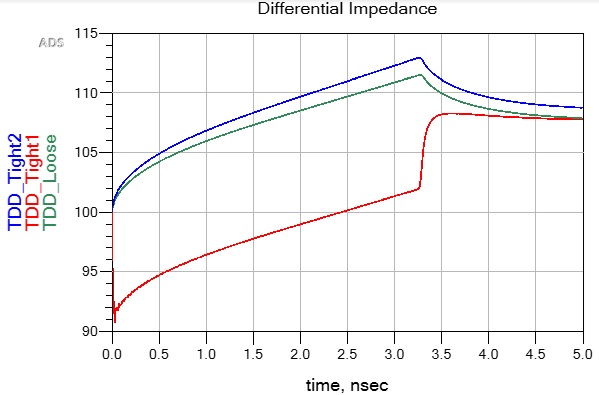
Figure 7. Differential TDR comparison of loose coupling (green); Tight1 coupling without line width adjustments (red) and Tight2 coupling with line width adjustment (blue).
To summarize then, it doesn’t matter if a differential pair is tightly coupled or loosely coupled. Properly engineered, both can be designed to properly match the output driver impedance. But as we have seen, each will have advantages and disadvantages.
Tighter coupling gives you better routing density at the expense of higher loss. Loose coupling allows for easier routing around obstacles and less loss. But in either case, they must be designed and measured for differential impedance.
So why is this important?
PCB fabrication shops use impedance as a metric to determine if the board has been fabricated to specification. Because the odd-mode impedance of a tightly spaced pair of traces depends on driving both traces differentially, you will not be able to determine the differential impedance by just measuring SE impedance of a tightly coupled pair like you could with two uncoupled traces.
References:
-
E. Bogatin, “Signal Integrity Simplified”, 3rd edition, Prentice Hall PTR, 2018
-
Keysight Advanced Design System (ADS) [computer software], (Version 2020)
-
Polar Instruments Si9000e [computer software] Version 2017
Simonovich-Cannonball Conductor Roughness Model Demystified
Recently on the SI-List there was great debate on whether or not my Cannonball model can be used to determine surface ratio and radius of sphere parameters needed for Huray roughness model from data sheets alone.
The author of this paper, “Conductor surface roughness modeling: From “snowballs” to “cannonballs”, [1] argues it is impossible to accurately model transmission lines from data sheets alone and seems to imply that because I had measured data in advance that I had magically “adjusted” Rz parameter to get such good correlation to measurements in my EDICon 2016 paper, “Practical Model of Conductor Surface Roughness Using Cubic Close-packing of Equal Spheres” [5].
Unfortunately his paper has created more confusion than clarity. To be clear, there is only ONE “Cannonball” model, and it is based on the cubic close packing of equal spheres, also known as face-centered cubic (FCC) packing.
The author of [1] also advocates using a material model identification methodology, similar to what I like to call the Design Feedback Method, shown in Figure 1. The author believes it is the only “accurate” way of determining printed circuit board (PCB) material properties for modeling.

Figure 1 Design Feed Back Method flow chart
This involves designing, building and measuring a test coupon with the intended PCB trace geometry to be used in final design. After modeling and tuning various parameters to best fit measured data, material parameters are extracted and then used in channel modeling software to design the final product.
The problem with this approach for many small companies is: TIME, RESOURCES, and MONEY.
-
Time to define stackup and test structures.
-
Time to actually design a test coupon.
-
Time to procure raw material – can take weeks, depending on scarcity of core/prepreg material.
-
Time to fabricate the bare PCB.
-
Time to assemble and measure.
-
Time to cross-section and measure parameters.
-
Time to model and fit parameters to measurements.
Then there is the issue of resources, which include having the right test equipment and trained personnel to get trusted measurements.
In the end this process ultimately costs more money, and material properties are only accurate for the sample from which they were extracted for the software and roughness model used. There is no guarantee extracted parameters reflect the true material properties.
There will be variation from sample to sample built from the same fab shop and more so from different fab shops because they have a different etch line and oxide alternative process.
For example Figure 2 shows measurements from two boards of the same design. As you can see there are differences in both insertion loss and TDR plots. Which curve do we use to fit parameters for material extraction to use in simulations? How many do we have to build and test to get a statistical sample of reality? How much time will this take? And how much money will it cost, especially if several PCB stackup geometries are required?

Figure 2 Comparison of insertion loss and TDR measurements of two boards of the same design
But, as Eric Bogatin often likes to say, “Sometimes an OK answer NOW is better than a good answer late”. For many signal integrity engineers, and design consultants, like myself, have to come up with an answer sooner, rather than later for many reasons. And depending on the issue at hand, those answers may be good enough. This was the initial motivation for my research.
So where do we get these parameters? Often the only sources are from manufacturers’ data sheets alone. But in most cases, the numbers do not translate directly into parameters needed for the EDA tools.
This paper will revisit the Cannonball model as it applies to the CMP-28 reference platform from Wildriver Technology [14], and as part of it I will show:
-
How to determine effective dielectric constant (Dkeff) due to roughness from data sheets alone.
-
How to apply my simple Cannonball stack model to determine roughness parameters needed for Huray model from data sheets alone.
-
How to apply these parameters using Simbeor software [10].
-
How to pull it all together with a simple case study.
But before we get into it, it is important to give a bit of background on material properties and PCB fabrication process.
Electro-deposited Copper
Electro-deposited (ED) copper is widely used in the PCB industry due to its low cost. A finished sheet of ED foil has a matte side and drum side. The matte side is usually treated with tiny nodules and is the side bonded to the core laminate. The drum side is always smoother than the matte side. For high frequency boards, sometimes the drum side of the foil is treated instead and bonded to the core. In this case it is known as reversed treated foil (RTF).
IPC-TM-650-2.2.17A defines the procedure for determining the roughness or profile of metallic foils used on PCBs. Profilometers are often used to quantify the roughness tooth profile of electro-deposited copper.
Nodule treated tooth profiles are typically reported in terms of 10-point mean roughness (Rz). Some manufacturers may also report root mean square (RMS) roughness (Rq). For standard foil this is the matte side. For RTF it is the drum side. Most often the untreated, or prepreg side, reports average roughness (Ra) in manufacturers’ data sheets.
With the realization of roughness having a detrimental effect on insertion loss (IL), copper suppliers began providing very low profile (VLP) and ultra-low profile (ULP) class of foils. VLP foils have treated roughness profiles less than 4 μm while ULP foils are less than 2 μm. Other names for ULP class are HVLP or eVLP, depending on the foil manufacturer.
It is important to obtain the actual vendor’s copper foil data sheet used by the respective laminate supplier for accurate modeling.
Oxide/Oxide Alternative Treatment
In order to promote good adhesion of copper to the prepreg material during the PCB lamination process, the copper surface is treated with chemicals to form a thin, nonconductive film of black or brown oxide. The controlled oxidation process increases the surface area, which provides a better bond between the prepreg and the copper surface. It also passivates the copper surface to protect it from contamination.
Although oxide treatment has been used for many years, eventually the industry learned that the lack of chemical resistance resulted in pink ring, which is indicative of poor adhesion between copper and prepreg. This weakness has led to oxide alternative (OA) treatments which rely on some sort of etching process, but no oxide layer is formed.
With the push for smoother copper to reduce conductor loss, newer chemical bond enhancement treatments, working at the molecular level, were developed to maintain copper smoothness, yet still provide good bonding to the prepreg.
Since OA treatment is applied to the drum side of the foil during the PCB Fabrication process, the OA roughness numbers should be used instead of Ra specified in foil manufacturer’s data sheets. RTF foil is modeled differently and discussed later in the case study.
Tale of Two Data Sheets
Everyone involved in the design and manufacture of PCBs knows the most important properties of the dielectric material are the dielectric constant (Dk) and dissipation factor (Df ).
Using Dk / Df numbers for stackup design and channel modeling from “Marketing” data sheets, like the example shown in Figure 3, will give inaccurate results. These data sheets are easily obtained when searching laminate supplier’s web sites.

Figure 3 Example of a “Marketing” data sheet easily obtained from laminate supplier’s web site. Source Isola Group.
Instead, real or “Engineering” data sheets, which are used by PCB fabricators to design stackups, should be used for PCB interconnect modeling. These data sheets define the actual thickness, resin content and glass style for different cores and prepregs. They include Dk / Df over a wide frequency range; usually from 100 MHz-10GHz.

Figure 4 Example of an “Engineering” data sheet showing Dk/Df for different glass styles and resin content over frequency. Source Isola Group.
Effective Dk Due to Roughness
Many engineers assume Dk published is the intrinsic property of the material. But in actual fact, it is the effective dielectric constant (Dkeff) generated by a specific test method. When simulations are compared against measurements, there is often a discrepancy in Dkeff, due to increased phase delay caused by surface roughness.
Dkeff is highly dependent on the test apparatus and conditions of how it is measured. One method commonly used by many laminate suppliers is the clamped stripline resonator test method, as described by IPC-TM-650, 2.5.5.5, Rev C, Test Methods Manual.
The measurements are done under stripline conditions using a carefully designed resonant element pattern card made with the same dielectric material to be tested. As shown in Figure 5, the card is sandwiched between two sheets of unclad dielectric material under test. Then the whole structure is clamped between two large plates; each lined with copper foil and are grounded. They act as reference planes for the stripline.

Figure 5 Illustration of clamped stripline resonator test method, as described by IPC-TM-650, 2.5.5.5, Rev C, Test Methods Manual
This method assures consistency of product when used in fabricated boards. It does not guarantee the values directly correspond to design applications.
This is a key point to keep in mind, and here is why.
Since the resonant element pattern card and material under test are not physically bonded together, there are small air gaps between the various layers that affect measured results. The small air gaps result in a lower Dkeff than what is measured in real applications using foil with different roughness bonded to the same core laminate. This is the primary reason for phase delay discrepancy between simulation and measurements.
If Dk and Rz roughness parameters from the manufacturers’ data sheets are known, then the effective Dk due to roughness (Dkeff_rough) of the fabricated core laminate can be estimated by [2]:
Equation 1

where: Hsmooth is the thickness of dielectric from data sheet; Rz is 10-point mean roughness from data sheet; Dk is dielectric constant from data sheet
Most EDA tools include a wideband causal dielectric model. To use it, you must enter Dk and Df at a particular frequency. I found it is usually best to use the values near the Nyquist frequency of the baud rate.
Modeling Copper Roughness
“All models are wrong but some are useful”– a famous quote by George E. P. Box, who was a British statistician in the mid-20th century. The same can be said when using various roughness models.
For example many roughness models require RMS roughness numbers, but often Rz is the only number available in data sheets, and vice versa. If Rz is defined as the sum of the average of the five highest peaks and the five lowest valleys of the roughness profile over a sample length, and Rq is the RMS value of that profile, then the roughness can be modeled as a triangular profile with a peak to valley height equal to Rz, as illustrated in Figure 6.

Figure 6 Triangular roughness profile model with peak to valley height equal to 10-point mean roughness Rz.
If we define the RMS height of the triangular roughness profile is equal to ∆, then:
Equation 2

And likewise, if we assume ∆ ~ Rq, then:
Equation 3
![]()
Several modeling methods were developed over the years to determine a roughness correction factor (KSR). When multiplicatively applied to the smooth conductor attenuation (αsmooth), the attenuation due to roughness (αrough) can be determined by:
Equation 4
![]()
Huray Model
In recent years, the Huray model has found its way into popular EDA software due to the continually increasing need for better modeling accuracy. The model is based on a non-uniform distribution of spherical shapes resembling “snowballs” and stacked together forming a pyramidal geometry.
By applying electromagnetic wave analysis, the superposition of the sphere losses can be used to determine the total loss of the structure. Since the losses are proportional to the surface area of the roughness profile, an accurate estimation of a roughness correction factor (KSRH) can be analytically solved by [4]:
Equation 5

Although it has been proven to be a pretty accurate model, it relied on analysis of scanning electron microscopy (SEM) pictures of the treated surface and tuning of parameters for best fit to measured data. This is not a practical solution if all you have is roughness parameters from manufacturers’ data sheets.
Simonovich “Cannonball” Conductor Roughness Model (A.K.A. Cannonball-Huray Model)
Building upon the work already done by Huray, and using the Cannonball stack principle, the sphere radius and flat base area parameters are easily estimated solely from roughness parameters published in manufacturers’ data sheets.
As illustrated in Figure 7 there are three rows of equal sized spheres stacked on a square tile base. Nine spheres are on the first row, four spheres in the middle row, and one sphere on top. This stacking arrangement is known as close-packing of equal spheres, but more commonly known as the “Cannonball” stack due to the method used by sailors to stack actual cannonballs aboard ships.

Figure 7 Cannonball-Huray physical model. The height of the stack is the RMS height of the peak to valley profile equal to Rz from data sheets.
If we could peer into the stack and imagine a pyramid lattice structure connecting to the center of all the spheres, then the total height is equal the height of two pyramids plus the diameter of one sphere.
Given the height of the Cannonball stack (∆) is equal to the RMS value of the peak to valley roughness profile; then from method described in my earlier papers, determining the sphere radius (r ), from Rz found in data sheets, can be further simplified and approximated as [13]:
![]()
and base area (Aflat) as:
Equation 7
![]()
Because the model assumes the ratio of Amatte/Aflat = 1, and there are only 14 spheres, the original Cannonball-Huray model can be further simplified to:
Equation 8

where: KCH (f) = Cannonball-Huray roughness correction factor, as a function of frequency; δ (f) = skin-depth, as a function of frequency in meters; r = the radius of spheres in meters (Equation 6)
CMP28 Case Study Revisited
To test the accuracy of the model, stackup details and measured data from a CMP28 test platform, design kit, courtesy of Wildriver Technology, shown in Figure 8, was used for model validation. The PCB stackup is shown in Figure 9
Two different sets of S-parameter (s2p) files from a 2 inch and 8 inch single-ended (SE) stripline traces shown were used in this study. The original set of measurements, from my previous papers, and a second set provided as part of CMP-28 design kit from another PCB were used for model correlation.
The 6 inch transmission line segment S-parameter data was de-embedded using Ataitec ISD software [8] for both sets of data.

Figure 8 Photo of a portion of CMP-28 test platform courtesy of Wildriver Technology used for model validation.

Figure 9 CMP-28 PCB Stackup
The PCB was fabricated with Isola FR408HR 3313 core and prepreg, with 1 oz. RTF. Dk and Df at 10GHz were obtained from the FR408HR data sheet found on their web site and shown in Figure 10 & Figure 11.

Figure 10 Isola FR408HR data sheet used for core dielectric properties.

Figure 11 Isola FR408HR data sheet used for prepreg dielectric properties.
The foil used on FR408HR core laminates is MLS, Grade 3, controlled elongation RTF from Oak-matsui. Roughness Rz parameters for drum and matte sides are 120μin (3.048 μm) and 225μin (5.715μm) respectively for 1 oz. copper foil.

Figure 12 MLS RTF foil data sheet used on FR408HR laminate.
An oxide or oxide alternative (OA) treatment is usually applied to the copper surfaces prior to final PCB lamination. When it is applied to the matte side of RTF, it tends to smoothen the macro-roughness slightly. At the same time, it creates a surface full of microvoids which follows the underlying rough profile and allows the resin to fill in the cavities, providing a good anchor.
MultiBond MP from Macdermid Enthone is an example of an oxide alternative micro-etch treatment commonly used in the industry. Typically 50 μin (1.27μm) of copper is removed when the treatment is completed, depending on the board shop’s process control, as per Figure 13.
In a subsequent paper by J.A. Marshall, presented at IPC APEX 2015 titled, “Measuring Copper Surface Roughness for High Speed Applications” [11], there is data supporting the hypothesis that RTF roughness gets smoother after OA application.

Figure 13 Macdermid Enthone MultiBond MP data sheet reference from their web site.
Table 1 summarizes the PCB design parameters, dielectric material properties and copper roughness parameters obtained from respective manufactures’ data sheets.
Table 1 CMP-28 Test Board and Data Sheet Parameters
| Parameter | FR408HR/RTF |
| Dk Core/Prepreg | 3.65/3.59 @10GHz |
| Df Core/Prepreg | 0.0094/0.0095 @ 10GHz |
| Rz Drum side | 3.048 μm |
| Rz Matte side before Micro-etch | 5.715 μm |
| Rz Matte side after Micro-etch | 4.445 μm |
| Trace Thickness, t | 1.25 mil (31.7μm ) |
| Trace Etch Factor | 60 deg |
| Trace Width, w | 11 mils (279.20 μm) |
| Core thickness, H1 | 12 mils (304.60 μm) |
| Prepreg thickness, H2 | 10.6 mils (269.00 μm) |
| GMS trace length | 6 in (15.23 cm) |
From Table 1 and by applying Equation 1, Dkeff of core and prepreg due to roughness were determined to be:

Next, the Cannonball model’s sphere radiuses, for matte and drum side of the foil, were determined to be:

Because most EDA tools only allow a single value for the radius parameter, the average radius (ravg) was determined to be:
Equation 9

Simbeor electromagnetic software from Simberian Inc. [10] was used for modeling the transmission lines. It includes the latest and greatest dielectric and conductor roughness models, including the Huray-Bracken causal metal model.
Solution explorer pane and solution tree, as shown in Figure 14, allows you to edit and view solution data as a tree structure. All parameters from Table 1 were entered here.
Simbeor requires two parameters; roughness factor (RF1) and sphere radius (SR1). Because the Cannonball model always has N=14 spheres and base area (Aflat) is always 36r2, r2 cancels out and RF1 can be simplified to:
Equation 10

Sphere radius (SR1) is ravg = 0.225 as calculated from Equation 9.

Figure 14 Simbeor Solution Explorer Pane and Solution Tree
The wideband causal dielectric model option was used to model dielectric properties over frequency. Effective Dk due to roughness for core and prepreg, calculated above, were substituted instead of data sheet values. Standard copper resistivity of 1.724e-8 ohm-meter was used.
After the transmission lines were modeled and simulated, the S-parameter results were saved in touchstone format. Keysight ADS [5] was used for further simulation analysis and comparison.
Dkeff can be derived from phase delay. This is also known as time delay (TD) and is often used as a metric for simulation correlation accuracy for phase. TD, as a function of frequency, in seconds, is calculated from the unwrapped measured transmission phase angle, and is given by:
Equation 11

and:
Dkeff , as a function of frequency, is then given by:
Equation 12

where:c = speed of light (m/s); Length = length of conductor (m)
Figure 15 compares the simulated results vs measurement of a 6inch, de-embedded stripline trace. The red plots are measured from CMP-28 design kit data. The data was bandwidth limited to 35 GHz. The blue plots are the original measured data used in my previous paper [5]. The green plots are modeled with data sheet values only with oxide alternative treatment applied. SE IL is shown on the left and Dkeff is shown on the right. As can be seen, there is excellent correlation.

Figure 15 Measured vs simulated insertion loss (left) and Dkeff (right) with OA etch treatment applied.
The author of [1] suggests is that because I had the measured data, Rz was “adjusted” to show excellent results. What he is implying is my “adjusting” the roughness, due to the oxide treatment, was the reason for such good results, in spite of the fact Macdermid’s OA data sheet reports typical 50 μin of copper removal after treatment and data from [11] showing RTF gets slightly smoother after OA treatment.
So ok, let’s see what happens if I didn’t adjust the roughness due to OA treatment. Instead of using Rz matte side after micro-etch (4.445 μm ) roughness, we will use 5.715 μm from data sheet.
This will affect Dkeff of prepreg and average sphere radius ravg , so we will recalculate them:

And average radius is:

Figure 16 compares the simulated results vs measurement. The red plots are measured from CMP-28 design kit data. The blue plots are the original measured data used in my previous paper [5]. The green plots are modeled with data sheet values only without oxide alternative treatment applied. SE IL is shown on the left and Dkeff is shown on the right.
As can be seen, there is still excellent correlation with insertion loss even though OA was not considered. As expected using the rougher number would increase effective Dk. But in the end the TDR plots in Figure 17shows impedance change is negligible.

Figure 16 Measured vs simulated insertion loss (left) and phase delay (right) without OA etch treatment applied.

Figure 17 Measured vs simulated TDR plots with OA etch treatment (left) and without (right).
Summary and Conclusions
By using Cannonball-Huray model, with copper foil roughness and dielectric material properties obtained solely from respective manufacturers’ data sheets, practical PCB interconnect modeling for high-speed design is now achievable using commercial field-solving software employing Huray model.
Measured results from two different boards confirmed there are variations due to manufacturing that would affect material model extraction method accuracy.
When oxide alternative treatment was not considered, even though the matte side roughness of RTF gets smoothened during the PCB fabrication process, the simulated results still show excellent correlation to the original measured data from previous paper [5].
References
[1] Y. Slepnev, “Conductor surface roughness modeling: From “snowballs” to “cannonballs”.
[2] B. Simonovich, “A Practical Method to Model Effective Permittivity and Phase Delay Due to Conductor Surface Roughness”. DesignCon 2017, Proceedings, Santa Clara, CA, 2017
[3] L. Simonovich, “Practical method for modeling conductor roughness using cubic close-packing of equal spheres,” 2016 IEEE International Symposium on Electromagnetic Compatibility (EMC), Ottawa, ON, 2016, pp. 917-920. doi: 10.1109/ISEMC.2016.7571773.
[4] Huray, P. G. (2009) “The Foundations of Signal Integrity”, John Wiley & Sons, Inc., Hoboken, NJ, USA., 2009
[5] L.Simonovich, “Practical Model of Conductor Surface Roughness Using Cubic Close-packing of Equal Spheres”, EDICon 2016, Boston, MA
[6] Keysight Advanced Design System (ADS) [computer software], (Version 2017). URL: http://www.keysight.com/en/pc-1297113/advanced-design-system-ads?cc=US&lc=eng.
[7] Isola Group S.a.r.l., 3100 West Ray Road, Suite 301, Chandler, AZ 85226. URL: http://www.isola-group.com/
[8] Ataitec, URL: http://ataitec.com/products/isd/
[9] V. Dmitriev-Zdorov, B. Simonovich, I. Kochikov, “A Causal Conductor Roughness Model and its Effect on Transmission Line Characteristics”, DesignCon 2018 Proceedings, Santa Clara, CA, 2018
[10] Simberian Inc., 2629 Townsgate Rd., Suite 235, Westlake Village, CA 91361, USA, URL: http://www.simberian.com/
[11] John A. Marshall, “Measuring Copper Surface Roughness for High Speed Applications”, IPC APEX Expo 2015.
[12] Macdermid Enthone, Multibond MP, Inner Layer Oxide Alternative Bonding. URL: https://electronics.macdermidenthone.com/products-and-applications/printed-circuit-board/surface-treatments/innerlayer-bonding
[13] B. Simonovich, “PCB Interconnect Modeling Demystified”. DesignCon 2019, Proceedings, Santa Clara, CA, 2019.
[14] Wild River Technology LLC 8311 SW Charlotte Drive Beaverton, OR 97007. URL: https://wildrivertech.com/
Via Stubs Demystified
 We worry about via stubs in high-speed designs because they cause unwanted resonant frequency nulls which appear in the insertion loss plot (IL) of the channel. But are all via stubs bad? Well, as with most answers relating to signal integrity, “It depends.”
If one of these frequency nulls happen to line up at or near the Nyquist frequency of the bit- rate (i.e. 1/2 of the bit-rate), the received eye will be devastated, resulting in a high bit-error-ratio (BER), or even link failure.
Figure 1 shows simulation results of two backplane channels. On the left are measured SDD21 insertion loss and eye diagram of a 10 GB/s, non-return-to-zero (NRZ) signal, with short through vias and long stubs ~ 270 mils. On the right, shows measured SDD21 IL and eye diagram of a channel with long through vias and shorter stubs ~ 65 mils
Because the ¼ -wave resonant null occurs at a frequency ~ 4. 4 GHz, this is near the Nyquist frequency for 10 GB/s. As can be seen, the eye is totally closed for the long stub case. But when the shorter stub case is simulated, the eye is open with plenty of margin.
So how does a via stub cause ¼ -wave resonance? This question can be explained with the aid of Figure 2. Starting on the left, we see a via with two sections. The through (thru) part is the top portion connecting a device pin to an inner layer trace of a printed circuit board (PCB). The stub portion is the lower portion and is an open circuit.
On the right a sinusoidal signal is injected into the pin at the top of the via and travels along the thru portion until it reaches the junction of the internal trace and stub. At that point, the signal splits. Some of it travels along the trace, and the rest continues down the stub. Once it reaches the bottom, it reflects back up. When it reaches the trace junction, it splits again with a portion traveling along the trace and the rest back to the source.
If f is the frequency of a sine wave, and the time delay (TD) through the stub portion equals a ¼ -wavelength, then when it reflects at the bottom and reaches the junction again, it will be delayed by ½ a cycle and cancels most of the original signal.

Figure 2 Illustration of a ¼ -wave resonance of a stub. If f = frequency where TD = ¼ wavelength, then when 2TD = ½ cycle minimum signal received.
Resonance nulls occurs at the fundamental frequency ( fo) and at every odd harmonic. If you know the length of the stub (in inches) and the effective dielectric constant (Dkeff), surrounding the via hole structure, the resonant frequency can be predicted by:
Equation 1

Where: fo is the ¼ -wave resonant frequency (GHz); c is the speed of light (~11.8 in/ns); Stub_length is inches.
You will find that Dkeff is not the same as the bulk Dk published in laminate manufacturers’ data sheets. It is typically higher. A higher Dkeff increases phase delay through the via resulting in a lower resonant frequency.
One reason is excess capacitance from the via pads as well as the via barrel’s proximity to the clearance hole openings (also known as anti-pads) in plane layers. The other is because of the anisotropic nature of the laminate material.
For the example in Figure 1, the ¼ -wave resonant frequency of the long via stub is ~ 4.4 GHz. With a stub length of ~ 270 mils, this gives a Dkeff of 6.16, which is considerably higher than the published bulk Dk of 3.65. When you model a via in an electro-magnetic (EM) 3D field solver, it automatically accounts for the excess capacitance, but you will still need to compensate for the anisotropic nature of the dielectric.
A material is anisotropic when there are different values for parallel (x-y) vs perpendicular (z) measured values for dielectric constant. Dielectric constant and loss tangent, as published in manufacturers’ data sheets, report perpendicular measured values. For FR-4 fiberglass reinforced laminates, anisotropy can range from 15% -25% higher. The bad news is these numbers are not readily available from data sheets.
For differentially driven vias with plane layers evenly distributed throughout the entire stackup, Dkeff can be roughly estimated by:
Equation 2

Where: Dkxy is the dielectric constant adjusted for anisotropy (15%-25% higher); Dkz is the bulk dielectric constant from data sheets; s is via-via spacing; drillØ is drill diameter; H and W are anti-pad shape dimensions as shown in Figure 3 .

Figure 3 Anti-pad parameters for Equation 2.
The effects of via stubs can be mitigated by: using blind or buried vias; back-drilling; or by using thru vias only (i.e. from top layer to bottom layer). Practically, the shortest stub that can be achieved by back-drilling is on the order of 5 to 10 mils.
As a rule of thumb, we usually strive to have an interconnect bandwidth (BW) to be five times the Nyquist frequency of the bit-rate. Since a ¼-wave resonant null behaves somewhat like a notch filter, depending on the high-frequency roll-off due to Q-factor, frequencies near resonance will be attenuated. For that reason a good rule of thumb to follow is making sure the first null should occur at the 7th harmonic, or higher, of the Nyquist frequency to maintain the integrity of the 5th harmonic frequency component that makes up the risetime of a signal.
With this in mind, for a given baud-rate (Baud) in GBd, the maximum stub length (lmax), in inches can be estimated by:
Equation 3

For NRZ signaling, the baud-rate is equal to the bit rate. But for pulse-amplitude modulation (PAM-4) signaling, which has 2 symbols per bit time, the baud-rate is ½ of that. Thus a 56 GB/s PAM-4 signal has a baud-rate of 28 GBd, and the Nyquist frequency is 14 GHz, which happens to be the same as 28 GB/s NRZ signalling.
Figure 4 presents a chart of maximum stub length vs baud-rate based on Equation 3, using a Dkeff = 6.16 (blue) vs 3.65 (red). It shows us the higher the baud-rate, the more the stub length becomes an issue, especially past 10 GBd. We also get a feel for the sensitivity of stub length to Dkeff . Even though there is ~ 70% difference in Dkeff, there is only ~ 30% delta in stub lengths for the same baud-rate. This means that even if we use the bulk Dk published in data sheets, we are probably not dead in the water.
If the respective stub length is greater than this, it does not mean there is a show stopper. Depending on how much longer means the eye opening at the receiver will be degraded and we lose margin. We see this by the example in Figure 1. Even though the stub lengths in the channel were almost double the value at 10 GBd from the chart, there is still plenty of eye opening.

Figure 4 Chart showing estimated maximum stub length vs baud-rate with Dkeff of 6.16 (red) vs 3.65 (blue) based on Equation 3
To further explore design space and test out the rule of thumb, a generic circuit model was built using Keysight ADS with the ability to vary the via stub lengths
Referring to the chart, at 28 GBd, the maximum stub length should be 12 mils, assuming a Dkeff of 6.16. Figure 5 shows simulation results for NRZ signalling. As can be seen, there was a difference of only 17 mV in eye height (1.5%), and no extra jitter for 12 mil stubs compared to 5 mil stubs.

Figure 5 Eye diagrams comparison with BER at 10E-12 for stub lengths of 5 mils vs 12 mils. Modeled and simulated with Keysight ADS.
But if we use the exact same channel model, and use the generic PAM-4 IBIS AMI model from Keysight Technologies, we can see the results plotted in Figure 6. On the left are the eye openings with 5 mil stubs and the right with 12 mil stubs. In this case, there was an average reduction of ~7 mV (6%) in eye heights, and 0.24 ps (2%) in eye widths at BER 10E-12 across all three eyes.

Figure 6 PAM-4, 28 GBd (56 GB/s) eye height and width comparison at BER of 10E-12 for 5 mil vs 12 mil stub lengths. Modeled and simulated with Keysight ADS.
Because PAM-4 signalling has three smaller eyes, that are one-third the size of an NRZ eye for the same amplitude, it is more sensitive to channel impairments. From the above examples, we can see NRZ had only 1.5% reduction in eye height compared to 6% for PAM-4. Similarly there was no increase in jitter for NRZ compared to 2% increase for PAM-4 when stub lengths changed from 5 mils to 12 mils.
What this says is maintaining a BW to 5 times Nyquist rule of thumb, when estimating via stub lengths, is quite conservative for NRZ signalling. There is almost the same BW as the channel with 5 mil stub, which was the original objective. But because PAM-4 is more sensitive to impairments, it shows there is less margin.
In summary then, rules of thumb and related equations are a good way to reinforce your intuitions or to give you an answer sooner rather than later. They help you know what to expect before you take any measurements or perform any simulations. But they should never be used to sign off on any high-speed design.
Because every system will have different impairments affecting BER, the only way to know how much margin you have is by modeling the via with a 3-D EM field solver, based on the actual stackup and simulating the entire channel complete with crosstalk, if margins are tight. This is even more critical for data rates above 10 GBd.
So to answer the original question, “are all via stubs bad”? Well, the answer is it still depends. For NRZ signalling, there is more leeway than for PAM-4. But you now have a practical way to quickly quantify the answer if you know the stub length, baud-rate and delay through the via.
Obsessions with Conductor Surface Roughness – What’s the Dk Because of it?
 You know you have an obsession when you are flying 6 miles over Colorado; look out your window at the beautiful scenery; and all you can think about is how the rocky mountain topology reminds you of conductor surface roughness! Well call me obsessed because that’s exactly what I thought on my way to DesignCon 2017 in Santa Clara, CA.
For those of you who know me, you know that I have been researching practical methods to model conductor surface roughness, and its effect on insertion loss (IL). I have presented several papers on the subject over the last couple of years. It’s one of my pet projects. This year, at DesignCon, I presented a paper titled, “A Practical Method to Model Effective Permittivity and Phase Delay Due to Conductor Surface Roughness” .
Everyone involved in the design and manufacture of printed circuit boards (PCBs) knows one of the most important properties of the dielectric material is the relative permittivity (εr), commonly referred to as dielectric constant (Dk). But in reality, Dk is not constant at all. It varies over frequency as you will see later.
We often assume the value reported in manufacturers’ data sheets is the intrinsic property of the material. But in actual fact, it is the effective dielectric constant (Dkeff) generated by a specific test method. When you compare simulation against measurements, you will often see a discrepancy in Dkeff and IL, due to increased phase delay caused by surface roughness. This has always bothered me. For a long time I was always looking for ways to come up with Dkeff from data sheet numbers alone. Thus the obsession and motivation for my recent research work.
Since phase delay, also known as time delay (TD), is proportional to Dkeff of the material, my theory was that the surface roughness profile decreases the effective separation between parallel plates, thereby increasing the electric field (e-field) strength, resulting in additional capacitance, which accounts for an increase in effective Dk and TD.
The main focus of my paper was to prove the theory and to show a practical method to model Dkeff and TD due to surface roughness. By referencing Gauss’s Law for charged parallel plates, I confirmed mathematically, and through simulation, how the dielectric thickness and permittivity are interrelated to e-field and capacitance. I also revealed how the 10-point mean (Rz) roughness parameter can be applied to finally estimate effective Dkeff due to roughness. Finally I tested the method via case studies.
In his book, “Transmission Line Design Handbook”, Wadell defines Dkeff as the ratio of the actual structure’s capacitance to the capacitance when the dielectric is replaced by air.
Dkeff is highly dependent on the test apparatus and conditions of how it is measured. There are several methods used in the industry. One method that is commonly used by many laminate suppliers is called the clamped stripline resonator test method. It is described by IPC-TM-650, section 2.5.5.5, Rev C.
In short, this method rapidly tests dielectric material for permittivity and loss tangent, over an X-band frequency range of 8-12.4 GHz, in a production environment. It does not guarantee the values are accurate for design applications.
Here’s why:
The measurements are made under stripline conditions, using a carefully designed resonant element pattern card, made out of the same dielectric material to be tested. The card is sandwiched between two sheets of unclad dielectric material under test. The whole structure is then clamped between two large plates, lined with copper foils that are grounded.
Since the resonant element pattern card and material under test are not physically bonded together, there are small air gaps between the various layers affecting measured results. These air gaps are caused in part by:
- Removing the copper from the material under test, leaving the bare substrate, complete with the micro void imprint of the copper roughness.
- The air gap between resonant element pattern card and material under test, due to the copper thickness of the etch pattern.
- The roughness profile of the copper, on the resonant element pattern card and fixture’s grounded foil reference planes, are different than would be in practice, unless the same foil type is used.
If Dkeff and Rz roughness parameters from the manufacturers’ data sheets are known, then the effective Dk due to roughness (Dkeff_rough) of the fabricated core laminate can now be easily estimated by:

Where: Hsmooth is the thickness of dielectric from data sheet; Rz is 10-point mean roughness from data sheet; and Dkeff is the Dk from data sheet.
With reference to Figure 1, using Dkeff with rough copper model, as shown on the left, is equivalent to using Dkeff_rough, with smooth copper model, as shown on the right. Therefore all you need to do is use Dkeff_rough for impedance calculations, and any other numerical simulations based on surface roughness, instead of Dk published in data sheets.
It is as simple as that.

Figure 1 Effective Dk due to roughness model. Using Dkeff with rough copper model (left) is equivalent to using Dkeff_rough with smooth copper model (right).
For example, one case study I presented used measurements from a CMP28 modeling platform from Wild River Technology. The PCB was fabricated with FR408HR material and reverse treated foil (RTF). Keysight EEsof EDA ADS software was used for modeling and simulation. The results are shown in Figure 2.
The left graph shows results when data sheet values for core and prepreg were used. Dkeff measured (red) was 3.761, compared to simulated Dkeff (blue) of 3.626, at 10 GHz. This gave a delta of ~ 4%. But when the Dkeff_rough was used for core and prepreg the delta was within 1%.

Figure 2 Measured vs simulated Dkeff using FR408HR data sheet values for core and prepreg (left) and using Dkeff_rough (right). Modeled and simulated with Keysight EEsof EDA ADS software.
The paper shows in more detail how Equation 1 was derived, based on Gauss’ Law. In addition, I show how IL and phase delay is also improved when Dkeff_rough is used instead of data sheet values. You can download the paper titled, “A Practical Method to Model Effective Permittivity and Phase Delay Due to Conductor Surface Roughness”, and other papers on modeling conductor loss due to roughness from my web site.
Practical Conductor Roughness Modeling with Cannonballs

In the GB/s regime, accurate modeling of conductor losses is a precursor to successful high-speed serial link designs. Failure to model roughness effects can ruin you day. For example, Figure 1 shows the simulated total loss of a 40 inch printed circuit board (PCB) trace without roughness compared to measured data. Total loss is the sum of dielectric and conductor losses. With just -3dB delta in insertion loss between simulated and measured data at 12.5 GHz, there is half the eye height opening with rough copper at 25GB/s.
So what do cannon balls have to do with modeling copper roughness anyway? Well, other than sharing the principle of close packing of equal spheres, and having a cool name, not very much.
According to Wikipedia, close-packing of equal spheres is defined as “a dense arrangement of congruent spheres in an infinite, regular arrangement (or lattice)” [8]. The cubic close-packed and hexagonal close-packed are examples of two regular lattices. The cannonball stack is an example of a cubic close-packing of equal spheres, and is the basis of modeling the surface roughness of a conductor in this design note.

Figure 1 Comparisons of measured insertion loss of a 40 inch trace vs simulation. Eye diagrams show that with -3dB delta in insertion loss at 12.5GHz there is half the eye opening at 25GB/s. Modeled and simulated with Keysight EEsof EDA ADS software [14].
Background
In printed circuit (PCB) construction there is no such thing as a perfectly smooth conductor surface. There is always some degree of roughness that promotes adhesion to the dielectric material. Unfortunately this roughness also contributes to additional conductor loss.
Electro-deposited (ED) copper is widely used in the PCB industry. A finished sheet of ED copper foil has a matte side and drum side. The drum side is always smoother than the matte side.
The matte side is usually attached to the core laminate. For high frequency boards, sometimes the drum side of the foil is laminated to the core. In this case it is referred to as reversed treated (RT) foil.
Various foil manufacturers offer ED copper foils with varying degrees of roughness. Each supplier tends to market their product with their own brand name. Presently, there seems to be three distinct classes of copper foil roughness:
· Standard
· Very-low profile (VLP)
· Ultra-low profile (ULP) or profile free (PF)
Some other common names referring to ULP class are HVLP or eVLP.
Profilometers are often used to quantify the roughness tooth profile of electro-deposited copper. Tooth profiles are typically reported in terms of 10-point mean roughness (Rz ) for both sides, but sometimes the drum side reports average roughness (Ra ) in manufacturers’ data sheets. Some manufacturers also report RMS roughness (Rq ).
Modeling Roughness
Several modeling methods were developed over the years to determine a roughness correction factor (KSR ). When multiplicatively applied to the smooth conductor attenuation (αsmooth ), the attenuation due to roughness (αrough ) can be determined by:
Equation 1
![]()
The most popular method, for years, has been the Hammerstad and Jensen (H&J) model, based on work done in 1949 by S. P. Morgan. The H&J roughness correction factor (KHJ ), at a particular frequency, is solely based on a mathematical fit to S. P. Morgan’s power loss data and is determined by [2]:
Equation 2

Where:
KHJ = H&J roughness correction factor;
∆ = RMS tooth height in meters;
δ = skin depth in meters.
Alternating current (AC) causes conductor loss to increase in proportion to the square root of frequency. This is due to the redistribution of current towards the outer edges caused by skin-effect. The resulting skin-depth (δ ) is the effective thickness where the current flows around the perimeter and is a function of frequency.
Skin-depth at a particular frequency is determined by:
Equation 3

Where:
δ = skin-depth in meters;
f = sine-wave frequency in Hz;
μ0= permeability of free space =1.256E-6 Wb/A-m;
σ = conductivity in S/m. For annealed copper σ = 5.80E7 S/m.
The model has correlated well for microstrip geometries up to about 15 GHz, for surface roughness of less than 2 RMS. However, it proved less accurate for frequencies above about 5GHz for very rough copper [3] .
In recent years, the Huray model [4] has gained popularity due to the continually increasing data rate’s need for better modeling accuracy. It takes a real world physics approach to explain losses due to surface roughness. The model is based on a non-uniform distribution of spherical shapes resembling “snowballs” and stacked together forming a pyramidal geometry, as shown by the scanning electron microscope (SEM) photo in Figure 2.

Figure 2 SEM photograph of electrodeposited copper nodules on a matte surface resembling “snowballs” on top of heat treated base foil. Photo credit Oak-Mitsui.
By applying electromagnetic wave analysis, the superposition of the sphere losses can be used to calculate the total loss of the structure. Since the losses are proportional to the surface area of the roughness profile, an accurate estimation of a roughness correction factor (KSRH) can be analytically solved by [1]:
Equation 4

Where:
KSRH (f ) = roughness correction factor, as a function of frequency, due to surface roughness based on the Huray model;
Aflat= relative area of the matte base compared to a flat surface;
ai = radius of the copper sphere (snowball) of the ith size, in meters;
Ni = number of copper spheres of the ith size per unit flat area in sq. meters;
δ (f ) = skin-depth, as a function of frequency, in meters.
Simonovich-Cannonball Model
Using the concept of cubic close-packing of equal spheres, the radius of the spheres (ai ) and tile area (Aflat ) parameters for the Huray model can now be determined solely by the roughness parameters published in manufacturers’ data sheets.
Why is this important? Well, as my friend Eric Bogatin often says, “Sometimes an OK answer NOW! is more important than a good answer late”. For example, often during the architectural phase of a backplane design, you are going through some what-if scenarios to decide on a final physical configuration. Having a method to accurately predict loss from data sheets alone rather than go through a design feedback method, described in [7] can save an enormous amount of time and money.
Another reason is that it gives you a sense of intuition on what to expect with measurements to help determine root cause of differences; or sanitize simulation results from commercial modeling tools. If you are like me, I always like to have alternate ways to verify that I have used the tool properly.
Recalling that losses are proportional to the surface area of the roughness profile, the Cannonball model can be used to optimally represent the surface roughness. As illustrated in Figure 3, there are three rows of spheres stacked on a square tile base. Nine spheres are on the first row, four spheres in the middle row, and one sphere on top.

Figure 3 Cannonball model showing a stack of 14 uniform size spheres (left). Top and front views (right) shows the area (Aflat) of base, height (HRMS) and radius of sphere (r).
Because the Cannonball model assumes the ratio of Amatte/Aflat = 1, and there are 14 spheres, Equation 4 can be simplified to:
Equation 5

Where:
KSR (f ) = roughness correction factor, as a function of frequency, due to surface roughness based on the Cannonball model;
r = sphere radius in meters; δ (f ) = skin-depth, as a function of frequency in meters;
Aflat = area of square tile base surrounding the 9 base spheres in sq. meters.
In my white paper [16] the radius of a single sphere is:

And the area of the square flat base is:
![]()
You can approximate the RMS heights of the drum and matte sides by Equation 6 and Equation 7 below:
Equation 6

Where: Rz_drum is the 10-point mean roughness in meters.
Equation 7

Where: Rz_matte is the 10-point mean roughness in meters.
Practical Example
To test the accuracy of the model, board parameters from a PCBDesign007 February 2014 article, by Yuriy Shlepnev [5] was used. Measured data was obtained from Simbeor software design examples courtesy of Simberian Inc. [9]. The extracted de-embedded generalized modal S-parameter (GMS) data was computed from 2 inch and 8 inch single-ended stripline traces. They were originally measured from the CMP-28 40 GHz High-Speed Channel Modeling Platform from Wild River Technology [14].
 The CMP-28 Channel Modeling Platform, (Figure 4 left -credit Wild River Technology) is a powerful tool for development of high-speed systems up to 40 GHz, and is an excellent platform for model development and analysis. It contains a total of 27 microstrip and stripline interconnect structures. All are equipped with 2.92mm connectors to facilitate accurate measurements with a vector network analyzer (VNA).
The PCB was fabricated with Isola FR408HR material and reverse treated (RT) 1oz. foil. The dielectric constant (Dk) and dissipation factor (Df), at 10GHz for FR408HR 3313 material, was obtained from Isola’s isoStack® web-based online design tool [10]. This tool is a free, but you need to register to use it. An example is shown in Figure 5.
Typical traces usually have a trapezoidal cross-section after etching due to etch factor. Since the tool does not handle trapezoidal cross-sections in the impedance calculation, an equivalent rectangular trace width was determined based on a 2:1 etch-factor (60 deg taper). The as designed nominal trace width of 11 mils, and a 1oz trace thickness of 1.25 mils per isoStack® was used in the analysis.

Figure 5 Example of Isola’s isoStack® online software used to determine dielectric thicknesses, Dk, Df and characteristic impedance for the CMP-28 board.
The default foil used on FR408HR core laminates is MLS, Grade 3, controlled elongation RT foil. The roughness parameters were easily obtained from Oak-mitsui [11]. Reviewing the data sheet, 1 oz. copper roughness parameters Rz for drum and matte sides are 120μin (3.175 μm) and 225μin (5.715μm) respectively. Because this is RT foil, the drum side is the treated side and bonded to the core laminate.
An oxide or micro-etch treatment is usually applied to the copper surfaces prior to final lamination. This provides enhanced adhesion to the prepreg material. CO-BRA BOND® [12] or MultiBond MP [13] are two examples of oxide alternative micro-etch treatments commonly used in the industry. Typically 50 μin (1.27μm) of copper is removed when the treatment is completed. But depending on the board shop’s process control, this can be 70-100 μin (1.78-2.54μm) or higher.
The etch treatment creates a surface full of micro-voids which follows the underlying rough profile and allows the resin to squish in and fill the voids providing a good anchor. Because some of the copper is removed during the micro-etch treatment, we need to reduce the published roughness parameter of the matte side by nominal 50 μin (1.27 μm) for a new thickness of 175μin (4.443μm).
Figure 6 shows SEM photos of typical surfaces for MLS RT foil courtesy of Oak-mitsui. The left and center photos are the treated drum side and untreated matte side respectively. The right photo is a 5000x SEM photo of the matte side showing micro-voids after etch treatment.

Figure 6 Example SEM photos of MLS RT foil courtesy of Oak-mitsui. Left is the treated drum side and center is untreated matte side. SEM photo on the right is the matte side after etch treatment.
The data sheet and design parameters are summarized in Table 1. Respective Dk, Df, core, prepreg and trace thickness were obtained from the isoStack® software, shown in Figure 5. Roughness parameters were obtained from Oak-mitsui data sheet. Rz of the matte side after micro-etch treatment (Rz = 4.443μm) was used to determine KSR_matte .
Table 1 CMP-28 test board parameters obtained from manufacturers’ data sheets and design objective.
|
Parameter |
FR408HR |
|
Dk Core/Prepreg |
3.65/3.59 @10GHz |
|
Df Core/Prepreg |
0.0094/0.0095 @ 10GHz |
|
Rz Drum side |
3.048 μm |
|
Rz Matte side before Micro-etch |
5.715 μm |
|
Rz Matte side after Micro-etch |
4.443 μm |
|
Trace Thickness, t |
31.730 μm |
|
Trace Etch Factor |
2:1 (60 deg taper) |
|
Trace Width, w |
11 mils (279.20 μm) |
|
Core thickness, H1 |
12 mils (304.60 μm) |
|
Prepreg thickness, H2 |
10.6 mils (269.00 μm) |
|
GMS trace length |
6 in (15.23 cm) |
Keysight EEsof EDA ADS software [14] was used for modeling and simulation analysis. A new controlled impedance line (CIL) designer enhancement, in version 2015.01, makes modeling the transmission line substrate easy. Unlike earlier substrate models, the CIL model allows you to model trapezoidal traces.
Figure 7 is the general schematic used for analysis. There are three transmission line substrates; one for dielectric loss; one for conductor loss and the other for total loss without roughness.

Figure 7 Keysight EEsof EDA ADS generic schematic of controlled impedance line designer used in the modeling and simulation analysis.
Dielectric loss was modeled using the Svensson/Djordjevic wideband Debye model to ensure causality. By setting the conductivity parameter to a value much-much greater than the normal conductivity of copper ensures the conductor is lossless for the simulation. Similarly the conductor loss model sets the Df to zero to ensure lossless dielectric.
Total insertion loss (IL) of the PCB trace, as a function of frequency, is the sum of dielectric and rough conductor insertion losses.
Equation 8
![]()
To accurately model the effect of roughness, the respective roughness correction factor (KSR ) must be multiplicatively applied to the AC resistance of the drum and matte sides of the traces separately. Unfortunately ADS, and many other commercial simulators, do not allow access to these surfaces to apply the correction properly. The best you can do is to apply the average of (KSR_drum ) and (KSR_matte ) side to the smooth conductor loss (ILsmooth ), as described above.
The following are the steps to determine KSR_avg (f ) and total IL with roughness:
1. Determine HRMS_drum and HRMS_matte from Equation 6 and Equation 7.

2. Determine the radius of spheres for drum and matte sides:

3. Determine the area of the square flat base for drum and matte sides:

4. Determine KSR_drum (f ) and KSR_matte (f ) :

5. Determine the average KSR_drum (f ) and KSR_matte (f ):

6. Apply Equation 8 to determine total insertion loss of the PCB trace.
![]()
Summary and Results
The results are plotted in Figure 8. The left plot compares the simulated vs measured insertion loss for data sheet values and design parameters. Also plotted is the total smooth insertion loss (crosses) which is the sum of conductor loss (circles) and dielectric loss (squares). Remarkably there is excellent agreement up to about 30GHz by just using algebraic equations and published data sheet values for Dk, Df and roughness.
The plot shown on the right is the simulated (blue) vs measured (red) effective dielectric constant (Dkeff ), and is determined by the equations shown. As can be seen, the measured curve has a slightly higher Dkeff (3.76 vs 3.63 @ 10GHz) than published. According to [6], the small increase in the Dk is due to the anisotropy of the material.
When the measured Dkeff (3.76) was used in the model, for core and prepreg, the IL results shown in Figure 9 (left) are even more remarkable up to 50 GHz!

Figure 8 IL (left) for a 6 inch trace in FR408HR RTF using supplier data sheet values for Dk, Df and Rz. Effective Dk is shown right.

Figure 9 IL (left) for a 6 inch trace in FR408HR RTF and effective Dk (right).
Figure 10 compares the Cannonball model against the H&J model. The results show that the H&J is only accurate up to approximately 15 GHz compared to the Cannonball model’s accuracy to 50GHz.

Figure 10 Cannonball Model (left) vs Hammerstad-Jensen model (right).
Conclusions
Using the concept of cubic close-packing of equal spheres to model copper roughness, a practical method to accurately calculate sphere size and tile area was devised for use in the Huray model. By using published roughness parameters and dielectric properties from manufacturers’ data sheets, it has been demonstrated that the need for further SEM analysis or experimental curve fitting, may no longer be required for preliminary design and analysis.
When measurements from CMP-28 modeling platform, fabricated with FR408HR and RT foil, was compared to this method, there was excellent correlation up to 50GHz compared to the H&J model accuracy to 15GHz.
The Cannonball model looks promising for a practical alternative to building a test board and extracting fitting parameters from measured results to predict insertion loss due to surface roughness.
For More Information
If you liked this design note and want to learn more, or get more details on this innovative roughness modeling methodology, you can visit my web site, LAMSIM Enterprises.com , and download a copy of the white paper [16], or my award winning DesignCon 2015 paper, [1]. And while you are there, feel free to investigate my other white papers and publications.
If you would like more information on our signal integrity and backplane services, or how we can help you achieve your next high-speed design challenge, email us at: info@lamsimenterprises.com
References
[1] Simonovich, Bert, “Practical Method for Modeling Conductor Surface Roughness Using Close Packing of Equal Spheres”, DesignCon 2015 Proceedings, Santa Clara, CA, 2015, URL: http://lamsimenterprises.com/Copyright2.html
[2] Hammerstad, E.; Jensen, O., “Accurate Models for Microstrip Computer-Aided Design,” Microwave symposium Digest, 1980 IEEE MTT-S International , vol., no., pp.407,409, 28-30 May 1980 doi: 10.1109/MWSYM.1980.1124303 URL: http://ieeexplore.ieee.org/stamp/stamp.jsp?tp=&arnumber=1124303&isnumber=24840
[3] S. Hall, H. Heck, “Advanced Signal Integrity for High-Speed Digital Design”, John Wiley & Sons, Inc., Hoboken, NJ, USA., 2009
[4] Huray, P. G. (2009) “The Foundations of Signal Integrity”, John Wiley & Sons, Inc., Hoboken, NJ, USA., 2009
[5] Y. Shlepnev, “PCB and package design up to 50 GHz: Identifying dielectric and conductor roughness models”, The PCB Design Magazine, February 2014, p. 12-28. URL: http://iconnect007.uberflip.com/i/258943-pcbd-feb2014/12
[6] Y. Shlepnev, “Sink or swim at 28 Gbps”, The PCB Design Magazine, October 2014, p. 12-23. URL: http://www.magazines007.com/pdf/PCBD-Oct2014.pdf
[7] E. Bogatin, D. DeGroot , P. G. Huray, Y. Shlepnev , “Which one is better? Comparing Options to Describe Frequency Dependent Losses”, DesignCon2013 Proceedings, Santa Clara, CA, 2013.
[8] Wikipedia, “Close-packing of equal spheres”. URL: http://en.wikipedia.org/wiki/Close-packing_of_equal_spheres
[9] Simberian Inc., 3030 S Torrey Pines Dr. Las Vegas, NV 89146, USA. URL: http://www.simberian.com/
[10] Isola Group S.a.r.l., 3100 West Ray Road, Suite 301, Chandler, AZ 85226. URL: http://www.isola-group.com/
[11] Oak-mitsui 80 First St, Hoosick Falls, NY, 12090. URL: http://www.oakmitsui.com/pages/company/company.asp
[12] Electrochemicals Inc. CO-BRA BOND®. URL: http://www.electrochemicals.com/ecframe.html
[13] Macdermid Inc., Multibond. URL: http://electronics.macdermid.com/cms/products-services/printed-circuit-board/surface-treatments/innerlayer-bonding/index.shtml
[14] Keysight Technologies, EEsof EDA, Advanced Design System, 2015.01 software. URL: http://www.keysight.com/en/pc-1297113/advanced-design-system-ads?cc=US&lc=eng
[15] Wild River Technology LLC 8311 SW Charlotte Drive Beaverton, OR 97007. URL: http://wildrivertech.com/home/
[16] Simonovich, Bert, “Practical Method for Modeling Conductor Surface Roughness Using The Cannonball Stack Principle”, White Paper, Issue 1.0, April 8, 2015,
URL: http://lamsimenterprises.com/Copyright.html
The Poor Man’s PCB Via Modeling Methodology
You are a backplane designer and have been assigned to engineer a new high-speed, multi-gigabit serial link architecture from several line cards to multiple fabric switch cards across a backplane. These links must operate at 6GB/s day one and be 10GB/s (IEEE 802.3KR) ready for product evolution. The schedule is tight, and you need to come up with a backplane architecture to allow the rest of the program to progress on schedule.
 You come up with a concept you think will work, but the backplane is thick with over 30 layers. There are some long traces over 30 inches and some short traces of less than 2 inches between card slots. There is strong pressure to reuse the same connector you used in your last design, but your gut tells you its design may not be good enough for this higher speed application.
Finally, you are worried about the size and design of the differential via footprint used for the backplane connectors because you know they can be devastating to the quality of the received signal. You want to maximize the routing channel through the connector field, which requires you to shrink the anti-pad dimensions, so the tracks will be covered by the reference planes, but you can’t easily quantify the consequences on the via of doing so.
You have done all you can think of, based on experience, to make the vias as transparent as possible without simulating. Removal of non-functional pads on the inner layers, and planning to back-drill the connector via stubs will help, but is it enough? You know in the back of your mind the best way to answer these questions, and to help you sleep at night, is to put in the numbers.
So you decide to model and simulate the channel. But to do so, you need accurate models of the vias to plug into your favorite circuit simulator. But how do you get these? You have heard it all before; “for high-speed, the best way to model a via is with a 3D electro-magnetic field solver”. Although this might be true, what if you don’t have access to such a tool, because the cost is more than your company wants to spend, or because you don’t have the expertise nor the time to learn how to build a model you can trust to make a timely decision?
On top of that, 3D field solvers typically produce S-parameter behavioral models. Since they represent only one sample of a given construction, it is impossible to perform what-if, worst case, min/max analysis with a single behavioral model. Because of this, many iterations of the model are required; causing further delay in getting your answer.
A circuit model on the other hand, is a schematic representation of the actual device. For any physical structure, there can be more than one circuit model to describe it. All can give the same performance, up to some bandwidth. When run in a circuit simulator, it predicts a measurable performance of the structure. These models can be parameterized so that worst case analysis can be explored quickly.
The problem with a circuit model is that you often need a behavioral model to calibrate it, or need to use analytical equations to estimate the parameters. But, as my friend Eric Bogatin often says, “an OK answer NOW! is better than a great answer late”.
In the past, it was next to impossible to develop a circuit model of a differential via structure without a behavioral model to calibrate it. These behavioral models were developed through empirical formulas, measured data, or through the use of 3D EM field solvers.
Now, there is another way. I have nicknamed it, “The Poor Man’s PCB Via Modeling Methodology”. Here’s how it works.
Anatomy of a Differential Via Structure:
 An example of a differential via structure, shown in Figure 1, is representative of vias used to connect surface mounted components or backplane connectors to internal layer traces.
The via barrel is a plated through hole extending the entire length of a PCB stack-up. The outside diameter equals the drill diameter. The inside diameter is the finished hole size (FHS) after plating. Pads are used on layers to ensure there is sufficient copper for track attachment after drilling operation. When used in this fashion, they are referred to as functional pads. Anti-pads are the clearance holes in the plane layers allowing the via barrel to pass through them without shorting.
The via portion is the length of the barrel connecting one signal layer to another. It is often referred to as the through via since it is part of the signal net. The stub portion is the rest of the barrel extending to the outer layer of the PCB. In high-speed designs, a good rule of thumb to remember is that a via stub should be less than 300mils/BR in length; where BR is the bit rate in Gb/s.
Building a Simple Scalable Circuit Model:
 On close examination of Figure 2, a differential via structure can be represented by a twin-rod transmission line geometry with excess capacitance (shown in red) distributed over its entire length. The smaller the anti-pad diameter, the greater the excess capacitance. This ultimately results in lower via impedance, causing higher reflections.
In all high-speed serial link designs, it is common practice to remove all non-functional pads and to maximize the anti-pad clearance as much as practically possible. Oval anti-pads are often used in this regard to further mitigate excess via capacitance.
Figure 3 illustrates the equivalent circuit for a differential via that could be used in a channel topology simulation. Here it is modeled with Keysight ADS software using a coupled line transmission line model for each section. This equivalent circuit model can be scaled for any combination of layer transitions and integrated in any channel simulation scenario.
 Since the cross-section of the via is constant throughout its length, the differential impedance of all sections of the via are the same. We only need to know the physical length of each segment and the effective dielectric constant (Dkeff) to get the time delay of each segment.
When driven differentially, the odd-mode parameters of each via are of major importance. Since the even-mode parameters have no impact on differential performance, both odd and even-mode parameters are set to the same values in the model.
The challenge then is to calculate the odd mode impedance (Zodd), representing the individual via impedance (Zvia), of a differential via structure and the effective dielectric constant (Dkeff) based on its geometry. Simple equations are used to determine these parameters.
Developing the Equations:
Anti-pads can vary in size and shape. They can be anything from round, to oval around each via, or even a large oval surrounding both vias as illustrated in Figure 4. Square, or rectangular variations (not shown) are similar. 
Referring back to Figure 2, we see the structure of each via looks a lot like two coaxial transmission lines with the inner layer reference planes acting like a shield. Electrostatically this is a good approximation, but because the shield is not continuous, the magnetic fields are not contained like they are in a coaxial structure. Instead they behave more like magnetic fields around a twin-rod structure.
So here lies the secret in modeling a differential via. We take the best of both geometries to calculate the odd-mode impedance representing Zvia.
For inductance, we will use the odd-mode inductance formula from the twin-rod transmission line geometry to calculate Lvia :

Referring to Figure 4, we then calculate the odd-mode capacitance for Cvia derived from an approximate formula for an elliptic coaxial structure developed by M.A.R. Gunston in his book, “Microwave Transmission Line Impedance Data” . In the original formula, both shield (W’+b) and inner conductor (w+t) are elliptical in shape and are dimensioned as shown. When the anti-pads are circular, then ln[(W’+b) /(w+t)] reduces to just ln[b/t)]; which is the denominator in the Coax equation. If we use Gunston’s approximation to calculate Cvia, then the equation becomes:

Since conventional FR4 type laminates are fabricated with a weave of glass fiber yarns and resin, they are anisotropic in nature. Because of this, the dielectric constant value depends on the direction of the electric fields. In a multi-layer PCB, there are effectively two directions of electric fields.
The one we are most familiar with has the electric fields perpendicular to the surface of the PCB; as is the case of stripline shown here in Figure 5. The dielectric constant, designated as Dkz in this case, is normally the bulk value of the dielectric specified by the laminate manufacturer’s data sheet.
The other case has the electric fields running parallel to the surface of the PCB, as is the case when a signal propagates through a differential via structure. In this situation, the dielectric constant, designated as Dkxy, can be15-20% higher than Dkz .
Therefore, assuming a nominal 18% anisotropic factor, Dkxy = 1.18(Dkz)
Now that we have defined Lvia, Cvia and Dkavg, Zvia can be estimated using the following equation:

But we are not finished yet. We still need to determine the effective dielectric constant (Dkeff) in order to accurately model the delay through the via and stub portion. Without the correct value, the quarter-wave resonant nulls in the insertion loss plot, due to the stub length, cannot be accurately predicted. The value for Dkeff is determined based on how much the via’s odd-mode impedance is decreased due to the distributed capacitive loading of the anti-pads.
To help us with this task, we start with the twin-rod formula. The odd-mode impedance (Zodd) is half the differential impedance (Ztwin), and is expressed as:

By substituting Equation 1 for Zodd into the equation above, and solving for Dkeff we eventually come up with the following equation:

Validating the Model:
A simple 26 layer test vehicle was fabricated to compare the accuracy of the differential via circuit model to real vias. It consisted of two differential via pairs separated by 6 inches of 100 Ohm stripline differential pairs. Three sample via structures representing long, medium and short via stubs, as summarized in Figure 6, were measured using an Agilent N5230A VNA.
The differential vias had the following common parameters:
 Via drill diameter; D = 28 mils
Center to center pitch; s = 59 mils
Oval anti-pads= 53 mils x 73 mils
Dk of the laminate = 3.65
Anisotropy in Dkxy = 18%
Zvia = Zstub = 31.7 Ohms (per Equation 1)
Dkeff = 6.8 (per Equation 2)
Agilent ADS software was used to model and facilitate simulation correlation of the measured data as captured in Figure 7. This simple model accounts for the discontinuity of the long through section and the long stub section. The top half is the measured channel using an S-parameter file. The bottom half is a circuit model of the channel. Since the probes were not calibrated out, they are part of the device under test. The balun transformers are used to facilitate the display of the S-parameter and TDR results.
The comparison between the measured and simulated results of the insertion loss and TDR response for the three via stub cases using this simple approximation methodology is summarized in Figure 8. The insertion loss plots, in the frequency domain, are shown on the left, while the TDR plots are shown on the right.
The resonant nulls in the SDD21 plots are due to the stub lengths. As you can see, the longer the stub, the lower the resonant frequency null. If this null happens at the Nyquist frequency of the bit rate, the eye will be totally closed. This is why we back-drill them out after the board has been fabricated.
The simulation correlation is excellent up to about 12 GHz. The TDR plots show excellent impedance matching and delay for all three cases, while the simulated stub resonant frequencies match the measured frequencies very well. As you can see, these simple approximations for Dkeff and Zvia are perfectly adequate in providing a quick and accurate circuit model for differential through hole vias typically used in backplane applications.
Summary:
As illustrated, a simple twin-rod model (Figure 2) is used as the basis for a practical differential via circuit modeling methodology. By using Equation 1 and Equation 2, you can quickly determine the odd-mode impedance and effective dielectric constant needed for the circuit model.
Of course, you should use this methodology first as a rough starting point to quickly estimate the performance of your differential via design. If your worst case topology simulations show the performance is marginal, then it is worth while to invest the time and money to develop a 3D full wave model to perform a more accurate analysis.
On the other hand, if you find this approximation shows the vias have little impact on the channel performance, it may be of greater value for you to invest your time and money in resolving other critical issues with your design.
Try it the next time you are losing sleep over your design challenges.
For more Information:

If you liked this design note and want to learn more, or get more details on this innovative via modeling methodology, you can visit my web site, LAMSIM Enterprises.com , and download a copy of the white paper I wrote along with Eric Bogatin and Yazi Cao titled, “Method of Modeling Differential Vias” .
While you are there, feel free to investigate my other white papers and publications.
If you would like more information on our signal integrity and backplane services, or how we can help you achieve your next high-speed design challenge, email us at: info@lamsimenterprises.com.
UPDATE: In collaboration with Saturn PCB, I am pleased to announce my differential via equations above have been incorporated in a new impedance calculator available now in Saturn PCB Tool Kit software suite.
Twin-rod and Rod-over-plane Transmission Line Geometries
In my last Design Note on coaxial transmission geometry, I mentioned it was one of three unique cross-sectional geometries that have exact equations for inductance and capacitance. The other two are twin-rod and rod-over-plane. All three relationships assume the dielectric material is homogeneous and completely fills the space when there are electric fields.
A common application for twin-rod geometry is twin-lead ribbon cable; once used for RF transmission between antenna and TV sets. With the popularity of cable and satellite TV over the years, twin-lead has given way to coaxial cable due to its superior noise rejection and shielding effectiveness.
If we look at Figure1, we can see the electromagnetic field relationship of a twin-rod geometry when it is driven differentially. As current propagates along one rod, an equal and opposite current flows in the opposite direction along the other.
The right half of Figure 1 shows the magnetic-field loops and direction of rotation around each rod. Only one loop is shown for clarity, but the number of loops is a function of the amount of current and the length of the rods. The counter-rotating loops of current forms a virtual return at exactly one half of the space between the two rods. We call this a virtual return because if we were to put a conducting plane in the same position, the electromagnetic fields would look exactly the same.

Figure 1 Twin-rod geometry showing electromagnetic field relationship.
In his book, “Signal Integrity Simplified”, Eric Bogatin defines the loop inductance as, “the total number of field line loops around a conductor per amp of current”, and the loop self-inductance as, “the total number of field line loops around a conductor per amp of current in the same loop” . Applying these definitions to the figure, the loop inductance (L) is the inductance between the two rods, and the loop self-inductance (L/2) is the loop self inductance to the virtual return plane; equal to one half the loop inductance.
Likewise, the left half of Figure 1 shows the electric field with a capacitance (C) between the two rods, and twice the capacitance (2C) from each rod to the virtual return plane.
The relationships between capacitance, inductance and impedance of a twin-rod geometry are described by the following equations:

Where:
Ctwin = Capacitance between twin-rods – F
Ltwin = Loop Inductance between twin-rods – H
Zdiff = Differential impedance of twin-rods – Ω
Dk = Dielectric constant of material
Len = Length of the rods – inches
r = Radius of the rods – inches
s = Space between the rods – inches
Because the electro-magnetic fields create a virtual return plane at exactly one half of the spacing between the rods, each rod behaves like a single rod-over-plane geometry as illustrated in Figure 2.

Figure 2 Electromagnetic fields comparison of Twin-rod (left) vs. Rod-over-plane (right) geometries.
Whenever an AC current carrying conductor is in close proximity to a conducting plane, as is the case for rod-over-plane, some of the magnetic-field lines penetrate it. When the current changes direction, the associated magnetic-field lines also change direction; causing small voltages to be induced in the plane. These voltages create eddy currents, which in turn produce their own magnetic-fields.
Eddy current-induced magnetic-field line patterns look exactly like magnetic-field lines from an imaginary current below the plane; located the same distance as the real current above the plane. This imaginary current is called an image current, and has the same magnitude as the real current; except in the opposite direction [1]. The image current creates associated image magnetic-field lines in the opposite direction of the real field lines. As a result, the real magnetic-field lines are compressed between the rod and the plane. Since the rod-over-plane geometry has only one rod, the loop inductance is the same as the loop self-inductance.
For a twin-rod geometry, the odd mode capacitance is the capacitance of each rod to virtual return plane and is equal to twice the capacitance between rods.

Likewise, the odd mode inductance is the inductance of each rod to virtual return plane and equal to one half the inductance between rods.

The odd mode impedance of each rod is half of the differential impedance, and is equivalent to the rod-over-plane impedance.

[1] “Signal Integrity Simplified”, Eric Bogatin
Coaxial Transmission Line Geometry
The coaxial (coax) transmission line geometry, described by Figure 1, consists of a center conductor; imbedded within a dielectric material; surrounded by a continuous outer conductor; also known as the shield. All share the same geometric center axis; hence the name coaxial. It is common practice to transmit the signal on the center conductor, while the outer conductor provides the return path for current back to the source. The shield is usually grounded at both ends.

Figure 1 Example of a coaxial transmission line geometry and the electromagnetic
field patterns with respect to the current through the structure.
As the signal propagates along the transmission line, an electromagnetic field is set up between the outer surface of the center conductor and the inner surface of the shield. As illustrated in red, the electric E-field pattern sets the capacitance per unit length, and the magnetic H-field, in blue, sets the inductance. For the center conductor, the “X” represents current flowing into the page and the “.” (dots) within the shield ring is current flowing out of the page.
Figure 2 describes the magnetic-field relationship for a coax geometry. As current propagates along the center conductor, concentric magnetic-field lines (blue) are created in the direction as shown following the right hand rule.
 Whenever an AC current carrying conductor is in close proximity to a conducting plane, some of the magnetic-field lines penetrate it. If this plane totally surrounds the inner conductor, it becomes the outer conductor in a coax geometry, and some of the magnetic-field lines penetrate the entire circumference. When the current changes direction, the associated magnetic-field lines also change direction, causing small voltages to be induced in the outer conductor. These voltages create eddy currents, which in turn, produce their own magnetic-fields.
Eddy current-induced magnetic-field line patterns look exactly like magnetic-field lines (grey) from imaginary currents surrounding the outer conductor. These imaginary currents are referred to as image currents, and have the same magnitude as the real current; except they are in the opposite direction [1]. For simplicity, there are only eight image currents shown. But in reality, there are many more; forming a continuous loop of imaginary currents on a radius equal to twice the radius of the outer conductor to the center of the circle. The image currents create associated image magnetic-field lines in the opposite direction of the real field lines. As a result, the real magnetic-field lines are compressed and are entirely contained within the outer conductor.
The outer conductor thus forms a shield preventing external magnetic-fields from coupling noise onto the main signal and likewise, prevents its own magnetic field from escaping and coupling to other cables or equipment. This is why it is a popular choice for RF applications.
The nice thing about a coaxial transmission line is you can use equations to calculate the exact inductance and capacitance per unit length. There are only two other geometries that can do the same. They are, twin-rod and rod-over-plane; which I will cover at a later time in separate design notes.
The relationships between capacitance, inductance and impedance can be expressed by the following equations:

Where:
Ccoax = Capacitance – F
Lcoax = Inductance – H
Zo = Characteristic Impedance – Ohms
Dk = Effective Dielectric constant
Len = Length of the rods – inches
D1 = Diameter of conductor
D2 = Diameter of shield
The coaxial structure can be flexible or semi-rigid in construction. Flexible coax is used for cable applications; like distributing cable TV or connecting radio transmitters/receivers with their antennas. To achieve its flexibility, the shield is usually braided and is protected by an outer plastic sheathing. Being flexible, the same cable can be reconfigured for different equipment applications.
Semi-rigid coax, in comparison, employs a solid tubular outer shield, which yields 100% RF shielding, and enables the dielectric material and center conductor to maintain a constant spacing; even through bends. If you have ever worked on your automobile brakes, semi-rigid coax resembles the rigid brake lines routed through the chassis to the wheels. Semi-rigid coax is usually used for microwave applications where optimum impedance control is required. A bending tool is needed to form it to a consistent radius. After initial forming and installation, it is not intended to be flexed or reconfigured.
[1] “Signal Integrity Simplified”, Eric Bogatin
