Posts Tagged ‘Printed circuit board’
A Tale of Two Data Sheets: Part1
Originally published SI Journal April 26, 2022
When doing printed circuit board (PCB) stackup and signal integrity (SI) impedance modeling, we need to get the dielectric material properties from the right sources. One important parameter for accurate impedance modeling is relative permittivity (εr) of the dielectric material, otherwise known as dielectric constant (Dk). The best source is from laminate suppliers’ data sheets. Though there is an issue with these I like to think of as, “a tale of two data sheets.”
Marketing data sheets, like the example shown in Figure 1 [6], are easily found on laminate suppliers’ websites. They are meant for quick comparison of dielectric properties to narrow your search for the right laminate for your application. Dielectric properties on marketing data sheets include mostly thermal and mechanical properties, which are important for the physical structure of the material and how it will perform with other material properties in the stackup during processing.
But marketing data sheets are not representative of what is needed to design an actual stackup, or to do impedance and SI loss modeling. Depending on glass style, resin content, thickness, Dk, and dissipation factor (Df) will be different for different cores and prepreg thicknesses for the same laminate. Marketing data sheets usually only report a typical Dk/Df at fifty percent resin content and two or three frequency points. Thickness is not specified. Furthermore, Dk and Df are not constant over frequency. So, using numbers from these data sheets will lead to inaccurate impedance and phase delay results.
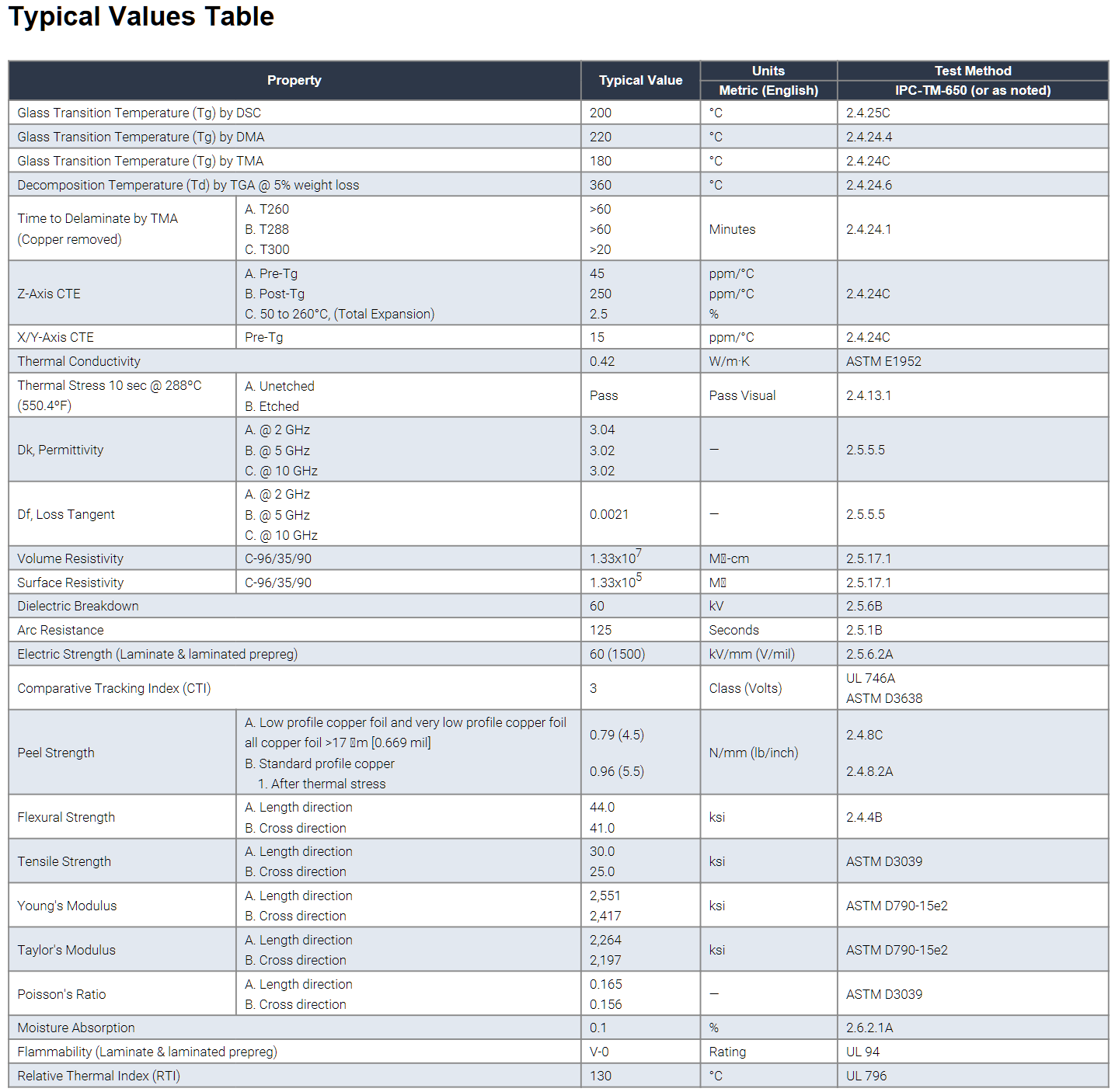
Figure 1. Example of a “Marketing” data sheet easily obtained from laminate supplier’s web site. Source Isola Group [6].
Instead, for transmission line modeling, one needs to use the same Dk/Df table data sheets PCB fabricators use to build the stackup. An example Dk/Df table is shown in Figure 2. Dk/Df tables provide the actual core and prepreg thicknesses, resin content, and Dk/Df for the different glass styles, over different frequencies. Depending on the stackup, a combination of thicknesses is often needed to meet impedance requirements. Each thickness will have a different Dk value.
In the example of Figure 2, Dk varies from 2.92 at 10 GHz for 1080 glass style to 3.19 at 10 GHz for 2116 glass style. This represents a Dk variation of -3.3% to 5.6% when compared to a Dk of 3.02 at 10 GHz specified in Figure 1.
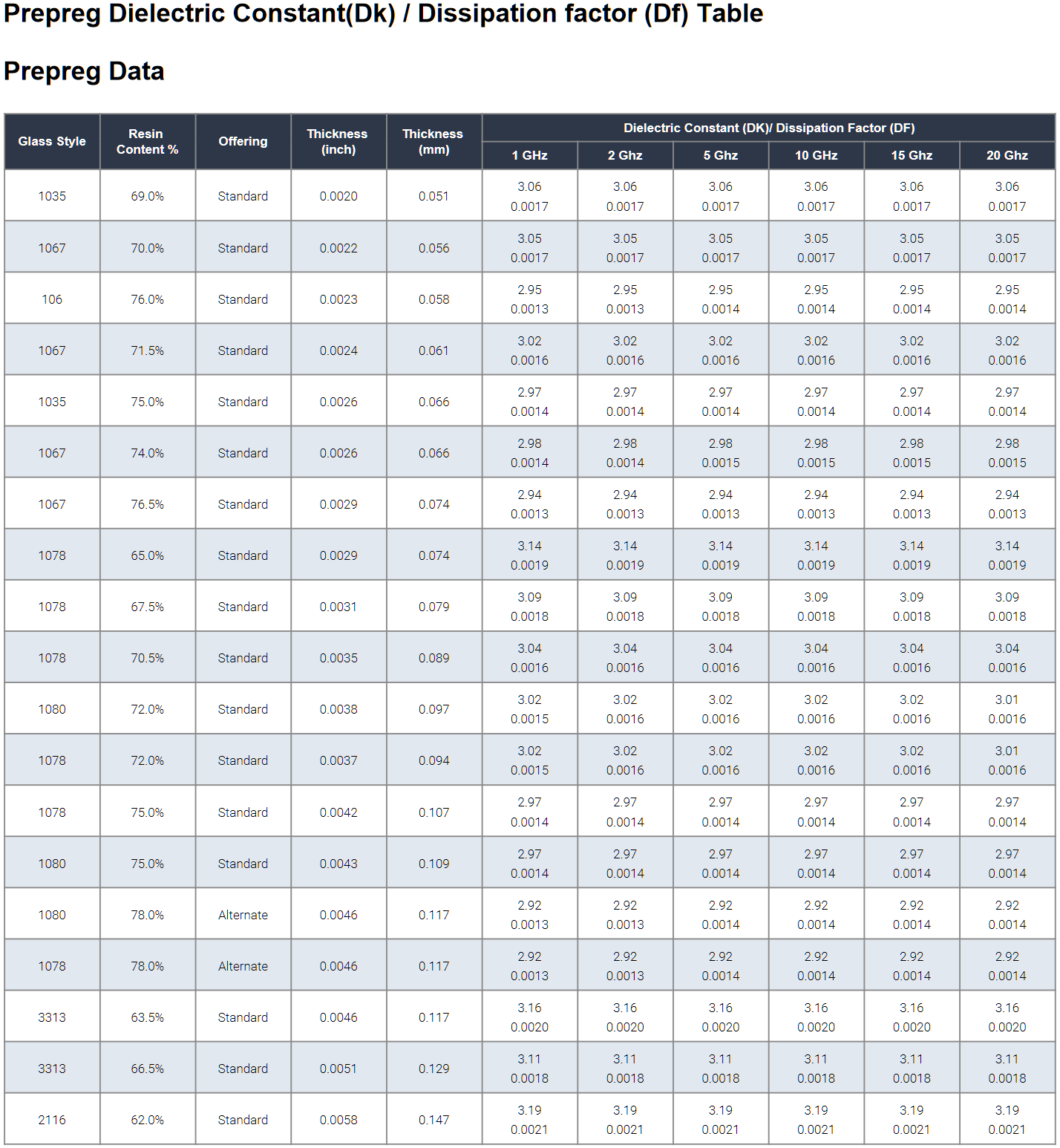
Figure 2. Example of a typical “Engineering” data sheet showing Dk/Df table for different glass styles and resin content over frequency. Source Isola Group [6].
Many engineers assume Dk published is the intrinsic property of the material. But, in fact, it is the effective Dk (Dkeff) measured by a specific industry standard test method. When they are compared against real measurements from a design application, there is often a discrepancy in Dkeff due to increased phase delay caused by surface roughness [1].
Dkeff is highly dependent on the test apparatus and conditions of how it is measured. One method commonly used by many laminate suppliers is the clamped stripline resonator test method, as described by IPC-TM-650 2.5.5.5, Rev C, Test Methods Manual [10].
Since all glass reinforced laminates are anisotropic, any stripline based test method, like TM-650 2.5.5.5, or Bereskin stripline test method [13], reports Dk values in which the E-fields are transverse to signal propagation. That is, if the signal propagation is in the x-y axis direction, then the Dk measured by this method is when E-fields are in the z-axis direction.
For Isola’s Dk/Df table [6], shown in Figure 2, Dk values were measured by TM-650 2.5.5.5 test method. From that data, the values for most of the constructions are calculated. Additional verification runs are performed to gather statistical data over time and validate that the calculations are reasonable and accurate.
The measurements are done under stripline conditions using a carefully designed resonant element pattern card. It is made with the same dielectric material to be tested. As shown in Figure 3, the card is sandwiched between two sheets of uncladded dielectric material under test. Then the whole structure is clamped between two large plates; each lined with copper foil and grounded. They act as reference planes for the stripline.
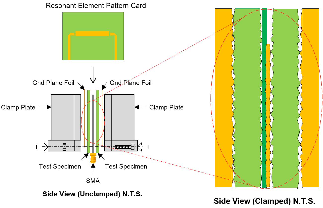
Figure 3. Illustration of clamped stripline resonator test method, as described by IPC-TM-650, 2.5.5.5, Rev C, Test Methods Manual [10].
This test method assures consistency of product when used in fabricated boards. It does not guarantee the values directly correspond to design applications.
Here is why:
Since the resonant element pattern card and material under test are not physically bonded together, air is entrapped between the various layers. These small air gaps are caused by the:
-
roughness of the copper foil plates in the fixture
-
roughness profile imprint left on the surface from the foil that was removed from the test samples
-
copper removed on the resonant element pattern card
Air entrapment, due to the TM-650 test method, is the primary reason for effective Dk and phase delay discrepancies between simulation using laminate suppliers’ Dk/Df tables and real measurements from a design application. The small air gaps result in a lower effective Dk than what would be measured in a real PCB because everything is pressed together with no air entrapment, as shown in a cross-section view of Figure 4.
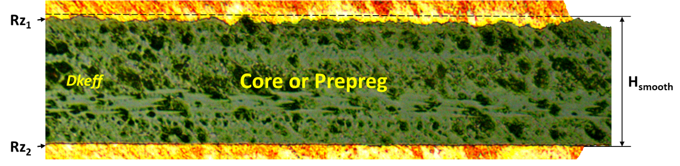
Figure 4. Example of foil bonded to core or prepreg dielectric. Rz1 is rougher than Rz2 and Hsmooth is the thickness of the dielectric as if the foil was removed.
When copper roughness is different on each side of the dielectric, like the example shown in Figure 4, Dkeff is determined heuristically by this simple correction factor:
Equation 1.
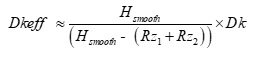
where:
-
Hsmooth is dielectric core thickness from laminate suppliers’ Dk/Df table data sheet or pressed prepreg thickness from the PCB stackup drawing.
-
Rz1 and Rz2 are the conductor roughness of the foil for the respective side of the dielectric from foil suppliers’ data sheet. Typically, Rz is the 10-point mean roughness as measured by a mechanical profilometer.
-
Dk is dielectric constant from laminate supplier’s Dk/Df table data sheet.
In Figure 4, Rz1 is the roughness of the top foil, and Rz2 is the roughness of the bottom foil. In this example, Rz1 is rougher than Rz2. Hsmooth is the core thickness of the dielectric, as specified in the Dk/Df table, or pressed thickness of the prepreg, often shown on a stackup drawing. It is the thickness of the dielectric as if the foil was removed.
When copper foil with the same Rz roughness is bonded to each side of the core or prepeg, Dkeff can be simplified as:
Equation 2
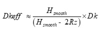
Figure 5 plots Dkeff over frequency derived from S21 phase or time delay (TD); Dkeff=(TDc0 ∕ length)2 from a Megtron-6 stripline case study [3]. This method is different than IPC-TM-650 test method in that it determines Dkeff from unwrapped phase delay rather than calculating Dk/Df from resonant peaks over the frequency range defined in the spec.
The blue plot is a simulated case based on core and prepreg Dk values from published Dk/Df tables at 12 GHz. When Dk is corrected due to roughness, using Equation 2, and resimulated, Dkeff is shown in pink. Although the Dkeff has improved, it still does not agree with the measured Dkeff from the device under test (DUT), shown in red.
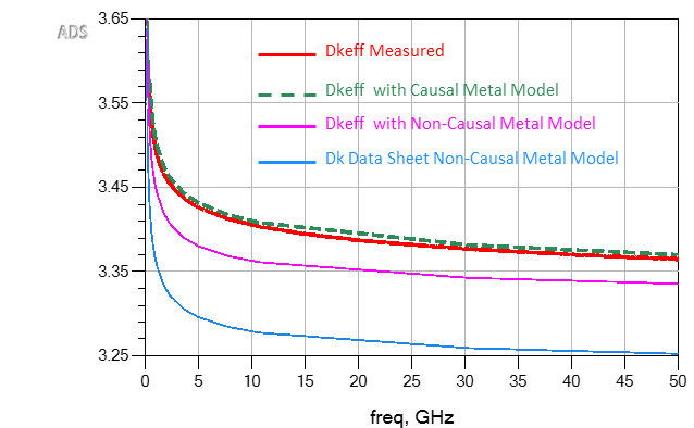
Figure 5. Comparisons of simulated Dkeff over frequency vs. measured. The red plot is actual measured Dkeff from the DUT. The middle pink plot is a simulation using Dkeff corrected due to roughness. The bottom blue plot is simulated using Dk at 12 GHz as published in Dk/Df tables and non-causal roughness model. The green dashed plot is a simulation using Dkeff due to roughness; a causal Huray-Bracken roughness model was used. Modeled with Simbeor [11] and simulated with Keysight ADS [12].
The discrepancy between the pink and red plots is because Dkeff from Equation 2 only corrects the phase delay due to self capacitance (C11) per unit length of the transmission line. But roughness of the foil also increases the self inductance (L11) per unit length of the transmission line, which adds additional phase or time delay [4].
This is counter intuitive and can be confusing since we usually relate Dkeff to capacitance only. By definition, Dkeff is the ratio of the actual structure’s capacitance to the capacitance when the dielectric is replaced by air. But this is only true for static electric fields. For time-variant electromagnetic fields, Dkeff becomes frequency-dependent [14].
If the propagation delay (tpd) for a single transmission line, in seconds per unit length, is determined by:
Equation 3.
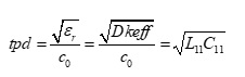
and c0 is the speed of light (~3.0E8 m/s) =1/sqrt(μ0 ε0 ); μ0 (4πE−7 H/m) and ε0 (8.8542E−12 F/m) is permeability and permittivity of free space respectively, then:
Equation 4.
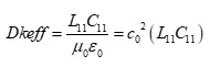
where: L11; C11 are self inductance in Henries per unit length and self capacitance in Farads per unit length respectively.
Equation 4 clearly shows that with an increase in self inductance there will be a proportional increase in Dkeff. This means for PCB transmission lines, calculating Dkeff=(TDc0 ∕ length)2 cannot be trusted to be the same as relative permittivity (εr) of the dielectric material. The consequence for doing so leads to inaccurate impedance predictions and non-causal time domain simulations, resulting in poor correlation to measurements.
A causal model, when simulated, does not produce any change in its output signal before there is a change in its input signal. When field solvers properly correct the self inductance, by applying the roughness correction factor to the imaginary portion of the complex impedance of the metal [4][5], the model is then causal. When combined with the corrected Dkeff for cores and prepregs from Equation 2, there is excellent correlation, as shown by the dashed green plot in Figure 5. Unfortunately, not all field solvers have causal roughness models to correct the inductance in the simulation.
Since there is no simple way to backtrack from a phase measurement to establish the right Dkeff to use for your modeling, especially for lossy stripline constructions, heuristic methods are an alternative.
Using the right Dkeff for your modeling ensures a correct time domain reflectometer (TDR) impedance prediction, as shown in Figure 6. The red plot is measured differential TDR from [3]. When core and prepreg Dk from Dk/Df tables were used along with a non-causal roughness model in the simulation, the blue plot shows an overestimate for impedance. When Dkeff from Equation 2, and a non-causal roughness model was used in the simulation, the pink plot shows an underestimate in the impedance plot.
It is only when we apply a causal Huray-Bracken roughness model from [11], along with Dkeff from Equation 2, that we see the effect of the increased self inductance, shown by the green dashed line plot in Figure 6.
At first glance of Figure 6, one might interpret the pink plot as having better correlation to the measured red plot. But because the measured plot has an impedance ripple along its length, it is difficult to conclude which is the correct model from the TDR plots alone. It is only when we compare Dkeff derived from the green dashed phase delay plot from Figure 5 that we can conclude the green dashed line TDR plot is the correct impedance.
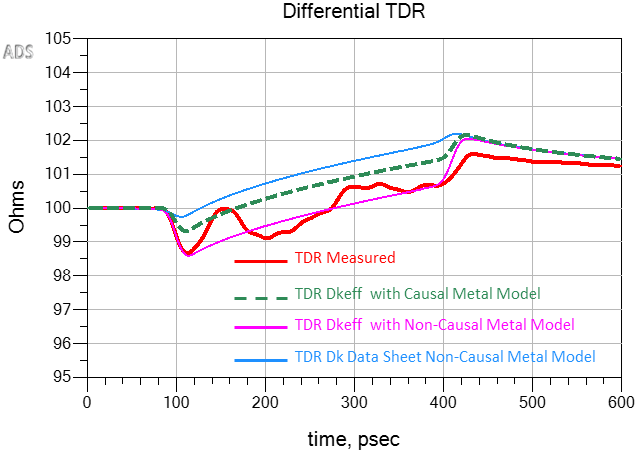
Figure 6. Simulated vs. measured differential TDR plots when different Dkeff was used in the model. The blue plot overestimates impedance when Dk from data sheets was used. The pink plot underestimates the impedance when Dkeff (Equation 2) and non-causal roughness model was used. The green dashed line plot is when Dkeff (Equation 2) and a causal Huray-Bracken roughness model were used. Modeled with Simbeor [11] and simulated with Keysight ADS [12].
Summary:
Dielectric constants from marketing data sheets cannot be trusted to properly design PCB stackups and model transmission lines for impedance and phase delay. Instead, laminate suppliers’ Dk/Df tables should be used.
Many laminate suppliers provide Dk/Df tables derived from a clamped stripline resonator test method [10] or similar Bereskin test method [13]. But the numbers do not factor the actual roughness of the foil. When a simple correction factor, based on the thickness of laminate and Rz foil roughness is considered, a more accurate value for Dkeff along with a causal roughness model can be used for impedance and transmission line modeling.
For PCB transmission lines, calculating Dkeff from phase or time delay measurement method cannot be trusted to be the relative permittivity of the dielectric material. Using this value will lead to inaccurate simulation results.
References:
1. L. Simonovich, “A Practical Method to Model Effective Permittivity and Phase Delay Due to Conductor Surface Roughness“, DesignCon 2017, Santa Clara, USA.
2. B. Simonovich, “Stackup Beware: Case Study of the Effects on Transmission Line Losses Due to Mixed Reference Plane Roughness”, Signal Integrity Journal article, August 10, 2021.
3. B. Simonovich, “PCB Fabrication: What SI/PI Engineers Need to Know for First Time Modeling Success”, DesignCon 2021 Spring Break Webinar Series, April 12-16, 2021.
4. V. Dmitriev-Zdorov, B. Simonovich, Igor Kochikov, “A Causal Conductor Roughness Model and its Effect on Transmission Line Characteristics“, DesignCon 2018, Santa Clara, USA.
5. J.E. Bracken, “A Causal Huray Model for Surface Roughness”, DesignCon 2012, Santa Clara, USA.
6. Isola Group, 6565 West Frye, Chandler, AZ 85226.
7. Circuit Foil, 6 Salzbaach, 9559 Wiltz, Grand Duchy of Luxembourg.
8. Rogers Corporation, 2225 W. Chandler Blvd., Chandler, AZ 85224.
9. J. Coonrod, “Managing PCB Materials: Dielectric Constant (Dk)”, Rogers Corporation, Blog Article, Sep 11, 2018
10. IPC-TM-650, 2.5.5.5, Rev C, Test Methods Manual
11. Simbeor THz [computer software].
12. Keysight ADS Keysight Advanced Design System (ADS) [computer software].
13. Bereskin, A. B. “Microwave Dielectric Property Measurements”, Microwave Journal, vol. 35, no.7, pp. 98 – 112
14. Wikipedia contributors. (2022, January 12). Relative permittivity. In Wikipedia, The Free Encyclopedia. Retrieved 18:14, January 14, 2022.
The Effects on Transmission Line Losses Due to Mixed Reference Plane Roughness Case Study
This article is an edited version of White Paper, “Heuristic Modeling of Transmission Lines due to Mixed Reference Plane Foil Roughness in Printed Circuit Board Stackups” [1].
Designing the right printed circuit board (PCB) stackup can make or break your product performance. If your product has circuitry that is transmission loss sensitive, then paying attention to conductor surface roughness is paramount.
Conductor surface roughness traditionally has been applied to copper foil to promote adhesion to the dielectric material. Early PCBs were only constructed with single or double-sided copper core laminates. The only important metric for copper was its purity and the roughness to improve peel strength. There was no such thing as a PCB stackup and nobody worried about impedance or transmission line losses.
But over the years PCBs have evolved into multi-layer constructions with evermore attention being paid to impedance control and transmission line losses. Thus a PCB stackup definition became vital for consistent performance.
Like any construction project, you need a blueprint before you start building. Similarly for PCBs, you need a stackup drawing and detailed fabrication notes. Part of the stackup design process includes signal integrity (SI) modeling for characteristic impedance and transmission loss. If your design is running at 56Gig pulse amplitude modulation level 4 (PAM-4), for example, you are probably looking at low loss dielectrics and low roughness copper for the signal traces.
But what is sometimes overlooked in the stackup, is the roughness of the reference planes. Often thin core laminate power and ground (GND) planes will specify reverse-treated foils (RTF), which are rougher on the side that bonds to the prepreg. Sometimes one of these planes, usually GND, acts as a reference plane to an adjacent signal layer as shown in Figure 1. If that adjacent high-speed signal layer is using smoother copper than one or both reference planes, a higher insertion loss than expected for that layer will occur and possibly ruin your day.
A similar scenario could occur for high density interconnect (HDI) technology. This is a popular method to increase component density on modern PCBs. By the nature of their stackup construction, a rougher copper reference plane could sometimes also end up adjacent to a signal layer as well. Thus, if insertion loss is a concern, copper foil roughness of reference planes needs to be considered.

Figure 1 An example cross-section stripline geometry from a stackup showing thin core laminate (top) with RTF bonded to prepreg and adjacent to a high-speed differential pair with smooth foil.
So how do you know this before you design your stackup and build your first prototype? Since we do not have any empirical data to go by, we can rely on a heuristic, high-level design (HLD) modeling method starting with published parameters found solely in manufacturer’s data sheets.
Heuristic HLD modeling is a practical technique that is not guaranteed to be perfect, but is still adequate in finding a satisfactory solution sooner, rather than later.
For dielectric parameters, we choose dielectric constant (Dk) / dissipation factor (Df) at or near the Nyquist frequency of the baud rate, then apply effective Dk (Dkeff) correction factor due to roughness, Equation 1 [5].

where:
H = thickness of core/prepreg; Rz is surface roughness of copper; Dk is as published in laminate supplier’s Dk/Df tables. Equation 1 assumes Rz of the foil on each side of the dielectric (core or prepreg) is the same.
For conductor loss, we use Rz roughness numbers from copper suppliers’ data sheets and oxide/oxide alternative Rz roughness numbers from your favorite fab shop, then apply the Cannonball-Huray roughness model [1]-[3].
Cannonball-Huray Model
The original Huray model is defined as:
Equation 2

The Cannonball-Huray model allows you to extract the right parameters using Rz roughness for core and prepreg sides of the foil [1]. Because the Cannonball-Huray model assumes the ratio of Amatte/Aflat = 1, and Ni = 14 spheres, the radius of a sphere (r) can be determined by:
![]()
and area of flat tile base (Aflat) by:
Equation 4

Wildriver Isola I-Tera® MT40 Custom Modeling Platform Case Study
To study the effect of reference plane roughness on transmission insertion loss, Wildriver Technology’s [7] custom modeling platform (CMP), shown in Figure 2, was used as a case study. This CMP was custom developed for Isola [6] to characterize their new I-Tera® MT40 very low-loss laminate material.
It combines 27 structures based on a consistent development of primitive structures; useful for performing a host of calibrations including automatic fixture removal, unknown THRU, WinCal XE™ calibration, and VNA gating and time transform analysis.

Figure 2 Wildriver Isola I-Tera® MT40 Custom Modeling Platform. Source: Wildriver Technology [7]
Stackup Validation
The PCB stackup is shown in Figure 3. Often PCB fab shop field application engineers (FAE) modify existing stackups and unintentionally make errors in transferring new parameters from data sheets into their software tools. Also, they may not necessarily know the design intent of the stackup. So the first step for any model correlation exercise is to sanitize the stackup, to ensure it meets the product design intent for signal integrity (SI) performance. In fact that is how the issue of different plane roughness was uncovered.
Since it is always a good practice to ensure the same roughness is specified for reference planes as the adjacent signal layers, I naively assumed it would be the case for any high-speed stackup. But that wasn’t the case here. Layers E1,E2 and E7, E8 specify 1oz RTF, while layers E3, E4 and E5, E6 specify 1oz VLP2 foil. Because the Isola I-Tera® MT40 CMP is intended to aid in modeling test structures, this is not a fatal flaw. On the contrary, it is a perfect platform to assess the effect of rougher reference planes.

Figure 3 Isola I-Tera® MT40 Custom Modeling Platform stackup. Source: Wildriver Technology [7]
Upon further review, it was discovered that the core laminates between E3,E4 and E5, E6 specified 1067/2×3313 glass styles, but this combination was not listed for 12 mil thickness. Instead, only 3×3313 core is offered. Because of that, the Dk shown is also wrong and will affect the impedance of the traces. The right Dk for 3×3313 is 3.53 instead if 3.33.
Foil Roughness
As mentioned earlier, the roughness of the foil affects the effective Dk, so we need to use the right number for our model validation. The standard VLP2 foil, used on I-Tera® MT40 core laminates is BF-TZA foil. Optional RTF foil, used for layers E1, E2 and E7, E8, is TWLS-B. Both are from Circuit Foil [8].
Relevant roughness parameters are shown in Figure 4. For the core side of the foil we are interested in the Rz parameters for the treated side listed in the table. But there are two Rz parameters, JIS B 601 and ISO 4287 specified. So which one do we use for modeling?
From IPC-TM-650 Section 1.2 [11] states, “The foil profile of foils shall be evaluated using the parameter Rz (DIN) or RTM, which is defined as the average maximum peak to valley height of five consecutive sampling lengths within the measurement length. This value is approximately equivalent to the values of profile determined from microsectioning techniques.”
and;
Section 1.3 states, “RZ (ISO) is a different parameter from Rz (DIN) and is not applicable to this method.”
Rz JIS represents the 10-point mean value, which is the sum of the average of the 5 highest peaks and the 5 lowest valleys over the sample length. Rz DIN is similar; except it is defined as the average maximum peak to valley height of five consecutive sampling lengths within the measurement length. Thus we will use Rz JIS for modeling analysis.

Figure 4 Roughness parameters from Circuit Foil [8] data sheets. Top is VLP2 standard foil used on I-Tera® MT40, while bottom is RTF option used for relevant layers in the stackup
Determine Effective Dk Due to Roughness
The first step in HLD impedance modeling is to gather all the dielectric and foil data sheet parameters to determine the effective Dk.
Figure 5 summarizes thickness of core, prepreg and signal trace from the stackup geometry in Figure 3. Note that photos are for illustrative purposes only and are not actual cross-sections from CMP PCB. Dk for core and prepreg were obtained from Isola I-Tera® MT40 Dk/Df tables [6].

Figure 5 Data sheet parameters for RTF/VLP2 foil roughness and dielectric properties for I-Tera® MT40 stackup geometry. Note: Photos are for illustrative purposes only and are not actual cross-sections from CMP PCB. Surface roughness pictures source: Circuit Foil [8]
The top reference plane is TWLS-B RTF foil with matte side 1 ≤ 7.5 JIS, obtained from Circuit Foil data sheet (Figure 4). The roughness surface profile is shown in the upper left. After OA smoothing, 1 ≤ 6.23 [1].
BF-TZA foil is used for both sides of the core laminate. The top surface of the stripline trace, shown in the upper right picture, is the drum side of the foil, before OA treatment. After OA treatment, Rz2 ~ 1.9 μm [1].
The bottom surface profile of the stripline trace and the top surface of the bottom reference plane are the treated matte sides of the foil, shown in the bottom right and bottom left pictures respectively. They both share the same roughness (Rz3, Rz4 =2.5μm JIS) from the BF-TZA data sheet (Figure 4).
The next step is to convert the imperial thickness units to metric, then use Equation 1 to determine Dkeff due to roughness for the prepreg and core.

Determine Cannonball-Huray Roughness Parameters
Several popular electronic design automation (EDA) tools include the Cannonball-Huray model directly as an option, so the respective Rz parameter is all that is needed.
Any of these tools can be used for HLD modeling, but my favorite is Polar SI9000 [9] because of its simplicity and sufficient accuracy for prefabrication modeling and analysis. Many fab shops use this tool for impedance prediction, so it is easy to stay in sync with them during the HLD stage of your project. Plus, it has the added benefit of modeling transmission loss and exporting S-parameters in touchstone format for further channel modeling in other tools.
Because Polar Si9000 assumes all the reference planes have the same roughness, it only allows Rz roughness parameters to be inputted for the matte and drum side of the signal trace. The best we can do, is take the average roughness of Rz1,Rz2 and Rz3,Rz4:

Simulation Correlation
When Dkeff due to roughness values were used instead of published Dk values, the new impedance prediction is 48.24 ohms, as shown in Figure 6.

Figure 6 Polar Si9000 impedance prediction with Dkeff due to roughness
Dkeff/Df for H1, H2 was then inputted into the causal dielectric model at 10GHz, as shown in Figure 7 (left), while Rzmatte, Rzdrum was inputted into the Cannonball-Huray model (right).

Figure 7 Causal Dkeff/Df dielectric and Cannonball-Huray roughness model input panels in Polar Si9000
After a 6-inch transmission line was simulated, the S-parameters were exported in touchstone format. Keysight Pathwave ADS [10] was used for further processing and analysis.
Figure 6 compares simulated insertion loss vs de-embedded reflectionless generalized modal (GM) S-parameter measurements, provided by Wildriver Technology [7]. As you can see there is excellent correlation without fitting to measured data!

Figure 8 HLD Insertion Loss simulation correlation for as designed stackup from data sheet and stackup parameters
Figure 9 plots simulated Dkeff vs measurements. At 10 GHz, simulated Dkeff is 0.105 (-2.8%) lower than measured value. Without actual cross-section microscopic measurements, it is difficult to conclude if the published Dk is wrong, or if there is process variation with roughness parameters used in the model.
But it is also interesting to note that measured Dkeff is not a constant value over frequency, as shown in the I-Tera® MT-40 Dk/Df tables. Instead Figure 9 reveals it varies over frequency, so the Dk/Df data sheet numbers are suspect.
Regardless, for the HLD modeling process, the simulation results are within acceptable tolerance.

Figure 9 HLD Dkeff simulation correlation for as designed stackup
Exploring the Effects of Alternate Foil Roughness
Now that we have good correlation to measurements, we can repeat the HLD modeling process to explore different foil roughness options. Figure 10 summarizes the thickness of core, prepreg and signal trace for VLP2/VLP2 foil (top) and VLP1/VLP1 foil (bottom). Note that photos are for illustrative purposes only and are not actual cross-sections from CMP PCB.
Respective Dkeff, and Cannonball-Huray roughness parameters were recalculated with same steps as VLP2/RTF case above.

Figure 10 Alternate foil options simulated for what-if loss comparison. Top is VLP2/VLP2 foil parameters for all copper layers and bottom is VLP1/VLP1 foil parameters for all copper layers. Note: Photos are for illustrative purposes only and are not actual cross-section from CMP PCB. Surface roughness pictures source: Circuit Foil [8]
Figure 11 presents the simulation results of all three scenarios. As expected. when the reference plane foil roughness went from RTF/VLP2 to VLP2/VLP2 there was improvement. At 14 GHz it was 0.5 dB and at 28GHz it was 1 dB improvement.
When VLP1/VLP1 foil was used, it was further improved by 0.8 dB and 1.7 dB at 14 GHz and 28 GHz respectively. So if your design is loss sensitive, you might want to consider VLP1 foil option.
When we compare Dkeff plots, we see effective Dk approaches actual Dk/Df data sheet values in the tables when smoother copper is used, as expected [5].
Since Dkeff was derived by phase delay, propagation delay will be affected by rougher copper.

Figure 11 What-if simulation comparison of VLP2/RTF, VLP2/VLP2, VLP1/VLP1 foil options and their effect on insertion loss and Dkeff
Conclusions
1. Roughness of reference planes make a significant difference in loss and phase delay, especially if one of the reference planes is RTF. If loss is important then all high-speed reference planes should have the same foil roughness specified
2. Heuristic HLD modeling method is a useful and accurate way to determine prefabrication impedance and loss predictions using data sheet parameters.
3. Published Dk from I-Tera® MT40 Dk/Df data sheet tables is not a flat constant over frequency.
4. Confirmed Rz JIS is the right parameter to use from Circuit Foil data sheet, instead of Rz ISO.
Acknowledgements
· Al Neves, CTO Wildriver Technology, for providing the custom modeling platform design details and measured data for the case study.
· Michael Gay, Director Business Development – Strategic Accounts at Isola Group, for providing foil supplier’s data sheets used on I-Tera® MT40 laminates.
References
[1] B. Simonovich, “Heuristic Modeling of Transmission Lines due to Mixed Reference Plane Foil Roughness in Printed Circuit Board Stackups”, White Paper, Lamsim Enterprises Inc.
[2] B. Simonovich, “Practical Method for Modeling Conductor Surface Roughness Using The Cannonball Stack Principle”, White Paper, Lamsim Enterprises Inc.
[3] L. Simonovich, “Practical method for modeling conductor roughness using cubic close-packing of equal spheres,” 2016 IEEE International Symposium on Electromagnetic Compatibility (EMC), 2016, pp. 917-920, doi: 10.1109/ISEMC.2016.7571773.
[4] L. Simonovich, “PCB Interconnect Modeling Demystified”, DesignCon 2019, Proceedings, Santa Clara, CA, 2019
[5] B. Simonovich, “A Practical Method to Model Effective Permittivity and Phase Delay Due to Conductor Surface Roughness”. DesignCon 2017, Proceedings, Santa Clara, CA, 2017
[6] Isola Group S.a.r.l., 3100 West Ray Road, Suite 301, Chandler, AZ 85226, URL: http://www.isola-group.com/
[7] Wild River Technology LLC 8311SW Charlotte Drive Beaverton, OR 97007, URL: https://wildrivertech.com/
[8] Circuit Foil 6 Salzbaach, 9559 Wiltz, Grand Duchy of Luxembourg URL: https://www.circuitfoil.com/portfolio/
[9] Polar Instruments Si9000e [computer software] Version 2018, URL: https://www.polarinstruments.com/index.html
[10] Keysight Pathwave Advanced Design System (ADS) [computer software], (Version 2021 update2). URL:http://www.keysight.com/en/pc-1297113/advanced-design-system-ads?cc=US&lc=eng.
[11] IPC-TM-650 Test Methods Manual 2.2.17A, Surface Roughness and Profile of Metallic Foils (Contacting Stylus Technique), 2/2001 Rev. A
[12] IPC-TM-650, 2.5.5.5, Rev C, Test Methods Manual
Practical Conductor Roughness Modeling with Cannonballs

In the GB/s regime, accurate modeling of conductor losses is a precursor to successful high-speed serial link designs. Failure to model roughness effects can ruin you day. For example, Figure 1 shows the simulated total loss of a 40 inch printed circuit board (PCB) trace without roughness compared to measured data. Total loss is the sum of dielectric and conductor losses. With just -3dB delta in insertion loss between simulated and measured data at 12.5 GHz, there is half the eye height opening with rough copper at 25GB/s.
So what do cannon balls have to do with modeling copper roughness anyway? Well, other than sharing the principle of close packing of equal spheres, and having a cool name, not very much.
According to Wikipedia, close-packing of equal spheres is defined as “a dense arrangement of congruent spheres in an infinite, regular arrangement (or lattice)” [8]. The cubic close-packed and hexagonal close-packed are examples of two regular lattices. The cannonball stack is an example of a cubic close-packing of equal spheres, and is the basis of modeling the surface roughness of a conductor in this design note.

Figure 1 Comparisons of measured insertion loss of a 40 inch trace vs simulation. Eye diagrams show that with -3dB delta in insertion loss at 12.5GHz there is half the eye opening at 25GB/s. Modeled and simulated with Keysight EEsof EDA ADS software [14].
Background
In printed circuit (PCB) construction there is no such thing as a perfectly smooth conductor surface. There is always some degree of roughness that promotes adhesion to the dielectric material. Unfortunately this roughness also contributes to additional conductor loss.
Electro-deposited (ED) copper is widely used in the PCB industry. A finished sheet of ED copper foil has a matte side and drum side. The drum side is always smoother than the matte side.
The matte side is usually attached to the core laminate. For high frequency boards, sometimes the drum side of the foil is laminated to the core. In this case it is referred to as reversed treated (RT) foil.
Various foil manufacturers offer ED copper foils with varying degrees of roughness. Each supplier tends to market their product with their own brand name. Presently, there seems to be three distinct classes of copper foil roughness:
· Standard
· Very-low profile (VLP)
· Ultra-low profile (ULP) or profile free (PF)
Some other common names referring to ULP class are HVLP or eVLP.
Profilometers are often used to quantify the roughness tooth profile of electro-deposited copper. Tooth profiles are typically reported in terms of 10-point mean roughness (Rz ) for both sides, but sometimes the drum side reports average roughness (Ra ) in manufacturers’ data sheets. Some manufacturers also report RMS roughness (Rq ).
Modeling Roughness
Several modeling methods were developed over the years to determine a roughness correction factor (KSR ). When multiplicatively applied to the smooth conductor attenuation (αsmooth ), the attenuation due to roughness (αrough ) can be determined by:
Equation 1
![]()
The most popular method, for years, has been the Hammerstad and Jensen (H&J) model, based on work done in 1949 by S. P. Morgan. The H&J roughness correction factor (KHJ ), at a particular frequency, is solely based on a mathematical fit to S. P. Morgan’s power loss data and is determined by [2]:
Equation 2

Where:
KHJ = H&J roughness correction factor;
∆ = RMS tooth height in meters;
δ = skin depth in meters.
Alternating current (AC) causes conductor loss to increase in proportion to the square root of frequency. This is due to the redistribution of current towards the outer edges caused by skin-effect. The resulting skin-depth (δ ) is the effective thickness where the current flows around the perimeter and is a function of frequency.
Skin-depth at a particular frequency is determined by:
Equation 3

Where:
δ = skin-depth in meters;
f = sine-wave frequency in Hz;
μ0= permeability of free space =1.256E-6 Wb/A-m;
σ = conductivity in S/m. For annealed copper σ = 5.80E7 S/m.
The model has correlated well for microstrip geometries up to about 15 GHz, for surface roughness of less than 2 RMS. However, it proved less accurate for frequencies above about 5GHz for very rough copper [3] .
In recent years, the Huray model [4] has gained popularity due to the continually increasing data rate’s need for better modeling accuracy. It takes a real world physics approach to explain losses due to surface roughness. The model is based on a non-uniform distribution of spherical shapes resembling “snowballs” and stacked together forming a pyramidal geometry, as shown by the scanning electron microscope (SEM) photo in Figure 2.

Figure 2 SEM photograph of electrodeposited copper nodules on a matte surface resembling “snowballs” on top of heat treated base foil. Photo credit Oak-Mitsui.
By applying electromagnetic wave analysis, the superposition of the sphere losses can be used to calculate the total loss of the structure. Since the losses are proportional to the surface area of the roughness profile, an accurate estimation of a roughness correction factor (KSRH) can be analytically solved by [1]:
Equation 4

Where:
KSRH (f ) = roughness correction factor, as a function of frequency, due to surface roughness based on the Huray model;
Aflat= relative area of the matte base compared to a flat surface;
ai = radius of the copper sphere (snowball) of the ith size, in meters;
Ni = number of copper spheres of the ith size per unit flat area in sq. meters;
δ (f ) = skin-depth, as a function of frequency, in meters.
Simonovich-Cannonball Model
Using the concept of cubic close-packing of equal spheres, the radius of the spheres (ai ) and tile area (Aflat ) parameters for the Huray model can now be determined solely by the roughness parameters published in manufacturers’ data sheets.
Why is this important? Well, as my friend Eric Bogatin often says, “Sometimes an OK answer NOW! is more important than a good answer late”. For example, often during the architectural phase of a backplane design, you are going through some what-if scenarios to decide on a final physical configuration. Having a method to accurately predict loss from data sheets alone rather than go through a design feedback method, described in [7] can save an enormous amount of time and money.
Another reason is that it gives you a sense of intuition on what to expect with measurements to help determine root cause of differences; or sanitize simulation results from commercial modeling tools. If you are like me, I always like to have alternate ways to verify that I have used the tool properly.
Recalling that losses are proportional to the surface area of the roughness profile, the Cannonball model can be used to optimally represent the surface roughness. As illustrated in Figure 3, there are three rows of spheres stacked on a square tile base. Nine spheres are on the first row, four spheres in the middle row, and one sphere on top.

Figure 3 Cannonball model showing a stack of 14 uniform size spheres (left). Top and front views (right) shows the area (Aflat) of base, height (HRMS) and radius of sphere (r).
Because the Cannonball model assumes the ratio of Amatte/Aflat = 1, and there are 14 spheres, Equation 4 can be simplified to:
Equation 5

Where:
KSR (f ) = roughness correction factor, as a function of frequency, due to surface roughness based on the Cannonball model;
r = sphere radius in meters; δ (f ) = skin-depth, as a function of frequency in meters;
Aflat = area of square tile base surrounding the 9 base spheres in sq. meters.
In my white paper [16] the radius of a single sphere is:

And the area of the square flat base is:
![]()
You can approximate the RMS heights of the drum and matte sides by Equation 6 and Equation 7 below:
Equation 6

Where: Rz_drum is the 10-point mean roughness in meters.
Equation 7

Where: Rz_matte is the 10-point mean roughness in meters.
Practical Example
To test the accuracy of the model, board parameters from a PCBDesign007 February 2014 article, by Yuriy Shlepnev [5] was used. Measured data was obtained from Simbeor software design examples courtesy of Simberian Inc. [9]. The extracted de-embedded generalized modal S-parameter (GMS) data was computed from 2 inch and 8 inch single-ended stripline traces. They were originally measured from the CMP-28 40 GHz High-Speed Channel Modeling Platform from Wild River Technology [14].
 The CMP-28 Channel Modeling Platform, (Figure 4 left -credit Wild River Technology) is a powerful tool for development of high-speed systems up to 40 GHz, and is an excellent platform for model development and analysis. It contains a total of 27 microstrip and stripline interconnect structures. All are equipped with 2.92mm connectors to facilitate accurate measurements with a vector network analyzer (VNA).
The PCB was fabricated with Isola FR408HR material and reverse treated (RT) 1oz. foil. The dielectric constant (Dk) and dissipation factor (Df), at 10GHz for FR408HR 3313 material, was obtained from Isola’s isoStack® web-based online design tool [10]. This tool is a free, but you need to register to use it. An example is shown in Figure 5.
Typical traces usually have a trapezoidal cross-section after etching due to etch factor. Since the tool does not handle trapezoidal cross-sections in the impedance calculation, an equivalent rectangular trace width was determined based on a 2:1 etch-factor (60 deg taper). The as designed nominal trace width of 11 mils, and a 1oz trace thickness of 1.25 mils per isoStack® was used in the analysis.

Figure 5 Example of Isola’s isoStack® online software used to determine dielectric thicknesses, Dk, Df and characteristic impedance for the CMP-28 board.
The default foil used on FR408HR core laminates is MLS, Grade 3, controlled elongation RT foil. The roughness parameters were easily obtained from Oak-mitsui [11]. Reviewing the data sheet, 1 oz. copper roughness parameters Rz for drum and matte sides are 120μin (3.175 μm) and 225μin (5.715μm) respectively. Because this is RT foil, the drum side is the treated side and bonded to the core laminate.
An oxide or micro-etch treatment is usually applied to the copper surfaces prior to final lamination. This provides enhanced adhesion to the prepreg material. CO-BRA BOND® [12] or MultiBond MP [13] are two examples of oxide alternative micro-etch treatments commonly used in the industry. Typically 50 μin (1.27μm) of copper is removed when the treatment is completed. But depending on the board shop’s process control, this can be 70-100 μin (1.78-2.54μm) or higher.
The etch treatment creates a surface full of micro-voids which follows the underlying rough profile and allows the resin to squish in and fill the voids providing a good anchor. Because some of the copper is removed during the micro-etch treatment, we need to reduce the published roughness parameter of the matte side by nominal 50 μin (1.27 μm) for a new thickness of 175μin (4.443μm).
Figure 6 shows SEM photos of typical surfaces for MLS RT foil courtesy of Oak-mitsui. The left and center photos are the treated drum side and untreated matte side respectively. The right photo is a 5000x SEM photo of the matte side showing micro-voids after etch treatment.

Figure 6 Example SEM photos of MLS RT foil courtesy of Oak-mitsui. Left is the treated drum side and center is untreated matte side. SEM photo on the right is the matte side after etch treatment.
The data sheet and design parameters are summarized in Table 1. Respective Dk, Df, core, prepreg and trace thickness were obtained from the isoStack® software, shown in Figure 5. Roughness parameters were obtained from Oak-mitsui data sheet. Rz of the matte side after micro-etch treatment (Rz = 4.443μm) was used to determine KSR_matte .
Table 1 CMP-28 test board parameters obtained from manufacturers’ data sheets and design objective.
|
Parameter |
FR408HR |
|
Dk Core/Prepreg |
3.65/3.59 @10GHz |
|
Df Core/Prepreg |
0.0094/0.0095 @ 10GHz |
|
Rz Drum side |
3.048 μm |
|
Rz Matte side before Micro-etch |
5.715 μm |
|
Rz Matte side after Micro-etch |
4.443 μm |
|
Trace Thickness, t |
31.730 μm |
|
Trace Etch Factor |
2:1 (60 deg taper) |
|
Trace Width, w |
11 mils (279.20 μm) |
|
Core thickness, H1 |
12 mils (304.60 μm) |
|
Prepreg thickness, H2 |
10.6 mils (269.00 μm) |
|
GMS trace length |
6 in (15.23 cm) |
Keysight EEsof EDA ADS software [14] was used for modeling and simulation analysis. A new controlled impedance line (CIL) designer enhancement, in version 2015.01, makes modeling the transmission line substrate easy. Unlike earlier substrate models, the CIL model allows you to model trapezoidal traces.
Figure 7 is the general schematic used for analysis. There are three transmission line substrates; one for dielectric loss; one for conductor loss and the other for total loss without roughness.

Figure 7 Keysight EEsof EDA ADS generic schematic of controlled impedance line designer used in the modeling and simulation analysis.
Dielectric loss was modeled using the Svensson/Djordjevic wideband Debye model to ensure causality. By setting the conductivity parameter to a value much-much greater than the normal conductivity of copper ensures the conductor is lossless for the simulation. Similarly the conductor loss model sets the Df to zero to ensure lossless dielectric.
Total insertion loss (IL) of the PCB trace, as a function of frequency, is the sum of dielectric and rough conductor insertion losses.
Equation 8
![]()
To accurately model the effect of roughness, the respective roughness correction factor (KSR ) must be multiplicatively applied to the AC resistance of the drum and matte sides of the traces separately. Unfortunately ADS, and many other commercial simulators, do not allow access to these surfaces to apply the correction properly. The best you can do is to apply the average of (KSR_drum ) and (KSR_matte ) side to the smooth conductor loss (ILsmooth ), as described above.
The following are the steps to determine KSR_avg (f ) and total IL with roughness:
1. Determine HRMS_drum and HRMS_matte from Equation 6 and Equation 7.

2. Determine the radius of spheres for drum and matte sides:

3. Determine the area of the square flat base for drum and matte sides:

4. Determine KSR_drum (f ) and KSR_matte (f ) :

5. Determine the average KSR_drum (f ) and KSR_matte (f ):

6. Apply Equation 8 to determine total insertion loss of the PCB trace.
![]()
Summary and Results
The results are plotted in Figure 8. The left plot compares the simulated vs measured insertion loss for data sheet values and design parameters. Also plotted is the total smooth insertion loss (crosses) which is the sum of conductor loss (circles) and dielectric loss (squares). Remarkably there is excellent agreement up to about 30GHz by just using algebraic equations and published data sheet values for Dk, Df and roughness.
The plot shown on the right is the simulated (blue) vs measured (red) effective dielectric constant (Dkeff ), and is determined by the equations shown. As can be seen, the measured curve has a slightly higher Dkeff (3.76 vs 3.63 @ 10GHz) than published. According to [6], the small increase in the Dk is due to the anisotropy of the material.
When the measured Dkeff (3.76) was used in the model, for core and prepreg, the IL results shown in Figure 9 (left) are even more remarkable up to 50 GHz!

Figure 8 IL (left) for a 6 inch trace in FR408HR RTF using supplier data sheet values for Dk, Df and Rz. Effective Dk is shown right.

Figure 9 IL (left) for a 6 inch trace in FR408HR RTF and effective Dk (right).
Figure 10 compares the Cannonball model against the H&J model. The results show that the H&J is only accurate up to approximately 15 GHz compared to the Cannonball model’s accuracy to 50GHz.

Figure 10 Cannonball Model (left) vs Hammerstad-Jensen model (right).
Conclusions
Using the concept of cubic close-packing of equal spheres to model copper roughness, a practical method to accurately calculate sphere size and tile area was devised for use in the Huray model. By using published roughness parameters and dielectric properties from manufacturers’ data sheets, it has been demonstrated that the need for further SEM analysis or experimental curve fitting, may no longer be required for preliminary design and analysis.
When measurements from CMP-28 modeling platform, fabricated with FR408HR and RT foil, was compared to this method, there was excellent correlation up to 50GHz compared to the H&J model accuracy to 15GHz.
The Cannonball model looks promising for a practical alternative to building a test board and extracting fitting parameters from measured results to predict insertion loss due to surface roughness.
For More Information
If you liked this design note and want to learn more, or get more details on this innovative roughness modeling methodology, you can visit my web site, LAMSIM Enterprises.com , and download a copy of the white paper [16], or my award winning DesignCon 2015 paper, [1]. And while you are there, feel free to investigate my other white papers and publications.
If you would like more information on our signal integrity and backplane services, or how we can help you achieve your next high-speed design challenge, email us at: info@lamsimenterprises.com
References
[1] Simonovich, Bert, “Practical Method for Modeling Conductor Surface Roughness Using Close Packing of Equal Spheres”, DesignCon 2015 Proceedings, Santa Clara, CA, 2015, URL: http://lamsimenterprises.com/Copyright2.html
[2] Hammerstad, E.; Jensen, O., “Accurate Models for Microstrip Computer-Aided Design,” Microwave symposium Digest, 1980 IEEE MTT-S International , vol., no., pp.407,409, 28-30 May 1980 doi: 10.1109/MWSYM.1980.1124303 URL: http://ieeexplore.ieee.org/stamp/stamp.jsp?tp=&arnumber=1124303&isnumber=24840
[3] S. Hall, H. Heck, “Advanced Signal Integrity for High-Speed Digital Design”, John Wiley & Sons, Inc., Hoboken, NJ, USA., 2009
[4] Huray, P. G. (2009) “The Foundations of Signal Integrity”, John Wiley & Sons, Inc., Hoboken, NJ, USA., 2009
[5] Y. Shlepnev, “PCB and package design up to 50 GHz: Identifying dielectric and conductor roughness models”, The PCB Design Magazine, February 2014, p. 12-28. URL: http://iconnect007.uberflip.com/i/258943-pcbd-feb2014/12
[6] Y. Shlepnev, “Sink or swim at 28 Gbps”, The PCB Design Magazine, October 2014, p. 12-23. URL: http://www.magazines007.com/pdf/PCBD-Oct2014.pdf
[7] E. Bogatin, D. DeGroot , P. G. Huray, Y. Shlepnev , “Which one is better? Comparing Options to Describe Frequency Dependent Losses”, DesignCon2013 Proceedings, Santa Clara, CA, 2013.
[8] Wikipedia, “Close-packing of equal spheres”. URL: http://en.wikipedia.org/wiki/Close-packing_of_equal_spheres
[9] Simberian Inc., 3030 S Torrey Pines Dr. Las Vegas, NV 89146, USA. URL: http://www.simberian.com/
[10] Isola Group S.a.r.l., 3100 West Ray Road, Suite 301, Chandler, AZ 85226. URL: http://www.isola-group.com/
[11] Oak-mitsui 80 First St, Hoosick Falls, NY, 12090. URL: http://www.oakmitsui.com/pages/company/company.asp
[12] Electrochemicals Inc. CO-BRA BOND®. URL: http://www.electrochemicals.com/ecframe.html
[13] Macdermid Inc., Multibond. URL: http://electronics.macdermid.com/cms/products-services/printed-circuit-board/surface-treatments/innerlayer-bonding/index.shtml
[14] Keysight Technologies, EEsof EDA, Advanced Design System, 2015.01 software. URL: http://www.keysight.com/en/pc-1297113/advanced-design-system-ads?cc=US&lc=eng
[15] Wild River Technology LLC 8311 SW Charlotte Drive Beaverton, OR 97007. URL: http://wildrivertech.com/home/
[16] Simonovich, Bert, “Practical Method for Modeling Conductor Surface Roughness Using The Cannonball Stack Principle”, White Paper, Issue 1.0, April 8, 2015,
URL: http://lamsimenterprises.com/Copyright.html
Are Guard Traces Worth It?
Originally published in, The PCB Design Magazine, April 2013 issue.
 By definition, a guard trace is a trace routed coplanar between an aggressor line and a victim line. There has always been an argument on whether to use guard traces in high-speed digital and mixed signal applications to reduce the noise coupled from an aggressor transmission line to a victim transmission line.
On one side of the debate, the argument is that the guard trace should be shorted to ground at regular intervals along its length using stitching vias spaced at 1/10th of a wavelength of the highest frequency component of the aggressor’s signal. By doing so, it is believed the guard trace will act as a shield between the aggressor and victim traces.
On the other side, merely separating the victim trace to at least three times the line width from the aggressor is good enough. The reasoning here is that crosstalk falls off rapidly with increased spacing anyways, and by adding a guard trace, you will already have at least three times the trace separation to fit it in.
In our DesignCon2013 paper titled, “Dramatic Noise Reduction using Guard Traces with Optimized Shorting Vias”, I coauthored along with Eric Bogatin, we showed that sometimes guard traces were effective, and sometime they were not; depending on how the guard trace was terminated. By correct management of the ends of the guard trace, we demonstrated it can reduce coupled noise on a victim line by an order of magnitude over not having the guard trace present. But if the guard trace was not optimized, the noise on the victim line can also be larger with the guard trace, than without.
Analysis Using Circuit Models
We started out the investigation by building circuit models for the topologies studied. Agilent’s EEsof EDS ADS software was used exclusively to model and simulate both stripline and microstrip configurations. The generic circuit model, with a guard trace, is shown in the top half of Figure 1. The circuit model, without a guard trace, is shown in the bottom half.
For the analysis, we used lossless transmission line models. The guard trace length was exactly matched to the coupled length. The ground stitching and the end-termination resistors, on the guard trace, could be deactivated, and/or shorted, as required. The line-width space geometry was set at 5-5-5 mils, and the spacing for the non-guarded topologies was set to three times the line width.

Figure 1 ADS schematic for generic topologies with a guard trace (top) and without (bottom). The transmission line were segmented and parameterized to easily change the lengths as required. The ground stitching and the end-termination resistors, shown in top schematic, can be deactivated and/or shorted as required.
Figure 2 is a summary of results when a guard trace was terminated in the characteristic impedance, left open, or shorted to ground at each end. The red waveforms are the results for topologies without a guard trace, and the blue waveforms are with a guard trace.
Depending on the nature of the termination, the reinfected noise on the guard trace can add or subtract to the directly coupled noise on the victim line. This often makes the net noise on the victim line worse than without a guard trace.
Unlike a simple two-line coupled model, where the near end crosstalk (NEXT) and far end crosstalk (FEXT) can be easily predicted from the RLGC matrix elements, trying to predict the same for a three-line coupled model is more difficult. Manually keeping track of all the noise induced on the guard trace, and its reinfection onto the victim line, is extremely tedious. First you must identify the directly coupled reinfected backward and forward noise on the victim line from the voltage on the guard trace. Then the problem is keeping track of the multiple reflections of the noise on the guard trace. Because of this, the only real way to analyse the effect is through circuit modeling and simulation.
In microstrip topologies, as you can see, there is little to no benefit to adding a guard trace; regardless of how the ends are terminated. This is because microstrip topologies are inherently prone to far end crosstalk. Therefore any far end noise, coupled onto the guard trace, will subsequently reinfect the victim with additional far end noise; as seen by the additional ringing superimposed on the blue waveform.
In stripline topologies, without a guard trace, there is no far-end cross talk generated. But when a guard trace is added, and depending on how the ends are terminated, any near end coupled noise on the guard trace can reinfect the victim. It is only when the ends are shorted to ground we see such a dramatic reduction of both near and far end noise.

Figure 2 Summary of simulation results when the ends of the guard trace was terminated, left open or shorted to ground for microstrip and stripline geometries.
Distributed Shorting Vias
When practically implementing a guard trace, to act as a shield, a rough rule of thumb suggests the spacing of shorting vias should be at least 1/10 the wavelength of the highest frequency content of the signal. For a risetime of 100 psec, the stitching via spacing, to meet l/10, is 0.18 inches; or 9 stitching vias over 1.5 inches.
Figure 3 summarizes the results when a guard trace was stitched to ground at multiple wavelengths; compared to the case of no guard. As you can see, in the case of microstrip, when the guard trace is shorted with fewer than 9 vias, there is still considerable ringing noise on the guard trace which can reinfect the victim line. But in the case of stripline, having two shorting vias at each end, or any number up to 9 shorting vias has the same result. This suggests there is no need for multiple shorting vias, other than at the end of the guard trace; as long as the guard trace is the same length as the coupled length. This dramatically simplifies the use of guard traces in stripline.

Figure 3 Summary of simulation results with guard trace stitched for microstrip and stripline geometries.
Practical Design Considerations
Up until now we have modeled and simulated ideal cases of shorting the guard traces to ground. But in reality, there are additional practical design considerations to consider. First is via size, and the impact it has on the line to line spacing. Next is the finite via inductance; since its impedance will prevent complete suppression of the noise on the guard trace. And finally, the extension of the guard trace compared to the coupled length.
Because through hole manufacturing design rules limit the smallest via and capture pads, the smallest mechanical drill size most PCB vendors will spec is 8 mils. By the time you factor in the minimum pad diameter and pad to copper spacing, the minimum space between the aggressor and victim lines would have to be at least 28 mils, as shown in Figure 4; just to fit a guard trace with grounding vias down its length.
At this point, you have to ask yourself if it is even worth it; especially for microstrip topologies. If the two signal lines were to be increased to 28 mils, the reduction in cross talk from just the added separation would likely be more significant than adding the shorted guard trace.

Figure 4 Minimum track to track spacing to fit an 8 mil drilled via and pad in through-hole technology.
Fortunately, the circuit analysis has shown there is little benefit to adding a guard trace to microstrip topologies, even if it was ground stitched appropriately. But to gain a dramatic reduction in cross talk in stripline all that is required is to short the guard trace at each end, and ensure the guard trace is exactly the same length as the coupled length. This means the minimum space to fit a via and guard trace can remain at three times the line width; as long as the guard trace is extended slightly, as shown in Figure 5(a). Alternatively, the guard trace can be made equal to the coupled length, as illustrated in Figure 5(b).
Agilent’s ADS Momentum planar 3D field solver was used to explore and quantify the implications vias and guard trace lengths have on noise reinfection. Figure 5 details a portion of the 3D model on the left end of the respective topologies. The right hand sides are identical. The reference planes are not shown for clarity.

Figure 5 Two examples of adding a grounded guard trace with minimum spacing of 3 x line width. Figure (a): guard trace is extended past the coupled length (A) by dimension B on both sides in order to satisfy minimum 5 mil pad-track spacing requirements. Figure (b): guard trace is equal to coupled length by separating the traces at each ends. Modeled in Agilent Momentum 3D field solver. Reference planes are not shown for clarity.
After simulation, the S-parameter data was saved in Touchstone format and brought into ADS for transient simulation analysis and comparison. Figure 6 shows the results. The plot on the left used 100 psec risetime for the step edge, while the plot on the right used 50 psec. Both plots are consistent with the dramatic noise reduction observed in Figure 2, except here we see some added noise ripple after about 0.8 nsec.
At 100 psec risetime, there is effectively no difference in near end noise signature for either (a) or (b) topology. But when the risetime was reduced to 50 psec, the noise ripple is more pronounced. The blue waveform shows that even when dimension B is 0 mils, there is still a small amount of noise due to the inductive length of the vias to the reference plane. The red waveform shows that adding just 12 mils to the guard trace length, at each end, the ripple magnitude is almost doubled.
It is a well-known fact that technology advancements over time results in faster and faster rise times. If you have engineered your design on the technology of the day, any future substitution of parts, with faster rise time, may cause your product to fail, or worse be intermittent.

Figure 6 Momentum transient simulation results comparing near end crosstalk at Port 1 when aggressor voltage was applied to Port 3. The red and blue waveforms are with a guard trace. The green waveform is with no guard and 15 mils separation. Aggressor voltage = 1V, 100 psec risetime (left) and 50 psec risetime(right)..
To explore this phenomenon, the guard trace was varied by 50 and 100 mils at each end, as illustrated in Figure 7. Here we can see that as the guard trace gets longer at each end, the noise ripple grows in magnitude quite rapidly. It is remarkable to note that when the guard trace is just 100 mils longer, at each end, the peak-peak amplitude of the noise just about equals the peak magnitude of the no guard case.

Figure 7 Momentum transient simulation results with guard trace extended. B = 12 mils (red), B = 50 mils (blue) and B = 100 mils (magenta) compared to no guard (green). Aggressor voltage = 1V, 100 psec risetime. Dimensions in mils.
When the guard trace was removed, and the space was increased to five times the line width, the near end crosstalk was reduced in magnitude and was approximately equal to the guard trace scenario, as seen in Figure 8. Furthermore, because there is no guard trace, there is no additional noise ripple.

Figure 8 Momentum transient simulation results comparing near end crosstalk at Port 1 when aggressor voltage was applied to Port 3. Aggressor voltage = 1V, 100 psec risetime.
So getting back to the original question, “Are guard traces worth it?” You be the judge. Using a guard trace, shorted at each end, can be effective, if you need the isolation. But it does have caveats. If you decide to go down this path, it is imperative for you to model and simulate your topology, preferably with a 3D field solver, before signing off on the design.
Reference
-
Eric Bogatin, Bert Simonovich,“Dramatic Noise Reduction using Guard Traces with Optimized Shorting Vias”, DesignCon2013, Santa Clara, CA, USA, Jan 28-31, 2013.
The Poor Man’s PCB Via Modeling Methodology
You are a backplane designer and have been assigned to engineer a new high-speed, multi-gigabit serial link architecture from several line cards to multiple fabric switch cards across a backplane. These links must operate at 6GB/s day one and be 10GB/s (IEEE 802.3KR) ready for product evolution. The schedule is tight, and you need to come up with a backplane architecture to allow the rest of the program to progress on schedule.
 You come up with a concept you think will work, but the backplane is thick with over 30 layers. There are some long traces over 30 inches and some short traces of less than 2 inches between card slots. There is strong pressure to reuse the same connector you used in your last design, but your gut tells you its design may not be good enough for this higher speed application.
Finally, you are worried about the size and design of the differential via footprint used for the backplane connectors because you know they can be devastating to the quality of the received signal. You want to maximize the routing channel through the connector field, which requires you to shrink the anti-pad dimensions, so the tracks will be covered by the reference planes, but you can’t easily quantify the consequences on the via of doing so.
You have done all you can think of, based on experience, to make the vias as transparent as possible without simulating. Removal of non-functional pads on the inner layers, and planning to back-drill the connector via stubs will help, but is it enough? You know in the back of your mind the best way to answer these questions, and to help you sleep at night, is to put in the numbers.
So you decide to model and simulate the channel. But to do so, you need accurate models of the vias to plug into your favorite circuit simulator. But how do you get these? You have heard it all before; “for high-speed, the best way to model a via is with a 3D electro-magnetic field solver”. Although this might be true, what if you don’t have access to such a tool, because the cost is more than your company wants to spend, or because you don’t have the expertise nor the time to learn how to build a model you can trust to make a timely decision?
On top of that, 3D field solvers typically produce S-parameter behavioral models. Since they represent only one sample of a given construction, it is impossible to perform what-if, worst case, min/max analysis with a single behavioral model. Because of this, many iterations of the model are required; causing further delay in getting your answer.
A circuit model on the other hand, is a schematic representation of the actual device. For any physical structure, there can be more than one circuit model to describe it. All can give the same performance, up to some bandwidth. When run in a circuit simulator, it predicts a measurable performance of the structure. These models can be parameterized so that worst case analysis can be explored quickly.
The problem with a circuit model is that you often need a behavioral model to calibrate it, or need to use analytical equations to estimate the parameters. But, as my friend Eric Bogatin often says, “an OK answer NOW! is better than a great answer late”.
In the past, it was next to impossible to develop a circuit model of a differential via structure without a behavioral model to calibrate it. These behavioral models were developed through empirical formulas, measured data, or through the use of 3D EM field solvers.
Now, there is another way. I have nicknamed it, “The Poor Man’s PCB Via Modeling Methodology”. Here’s how it works.
Anatomy of a Differential Via Structure:
 An example of a differential via structure, shown in Figure 1, is representative of vias used to connect surface mounted components or backplane connectors to internal layer traces.
The via barrel is a plated through hole extending the entire length of a PCB stack-up. The outside diameter equals the drill diameter. The inside diameter is the finished hole size (FHS) after plating. Pads are used on layers to ensure there is sufficient copper for track attachment after drilling operation. When used in this fashion, they are referred to as functional pads. Anti-pads are the clearance holes in the plane layers allowing the via barrel to pass through them without shorting.
The via portion is the length of the barrel connecting one signal layer to another. It is often referred to as the through via since it is part of the signal net. The stub portion is the rest of the barrel extending to the outer layer of the PCB. In high-speed designs, a good rule of thumb to remember is that a via stub should be less than 300mils/BR in length; where BR is the bit rate in Gb/s.
Building a Simple Scalable Circuit Model:
 On close examination of Figure 2, a differential via structure can be represented by a twin-rod transmission line geometry with excess capacitance (shown in red) distributed over its entire length. The smaller the anti-pad diameter, the greater the excess capacitance. This ultimately results in lower via impedance, causing higher reflections.
In all high-speed serial link designs, it is common practice to remove all non-functional pads and to maximize the anti-pad clearance as much as practically possible. Oval anti-pads are often used in this regard to further mitigate excess via capacitance.
Figure 3 illustrates the equivalent circuit for a differential via that could be used in a channel topology simulation. Here it is modeled with Keysight ADS software using a coupled line transmission line model for each section. This equivalent circuit model can be scaled for any combination of layer transitions and integrated in any channel simulation scenario.
 Since the cross-section of the via is constant throughout its length, the differential impedance of all sections of the via are the same. We only need to know the physical length of each segment and the effective dielectric constant (Dkeff) to get the time delay of each segment.
When driven differentially, the odd-mode parameters of each via are of major importance. Since the even-mode parameters have no impact on differential performance, both odd and even-mode parameters are set to the same values in the model.
The challenge then is to calculate the odd mode impedance (Zodd), representing the individual via impedance (Zvia), of a differential via structure and the effective dielectric constant (Dkeff) based on its geometry. Simple equations are used to determine these parameters.
Developing the Equations:
Anti-pads can vary in size and shape. They can be anything from round, to oval around each via, or even a large oval surrounding both vias as illustrated in Figure 4. Square, or rectangular variations (not shown) are similar. 
Referring back to Figure 2, we see the structure of each via looks a lot like two coaxial transmission lines with the inner layer reference planes acting like a shield. Electrostatically this is a good approximation, but because the shield is not continuous, the magnetic fields are not contained like they are in a coaxial structure. Instead they behave more like magnetic fields around a twin-rod structure.
So here lies the secret in modeling a differential via. We take the best of both geometries to calculate the odd-mode impedance representing Zvia.
For inductance, we will use the odd-mode inductance formula from the twin-rod transmission line geometry to calculate Lvia :

Referring to Figure 4, we then calculate the odd-mode capacitance for Cvia derived from an approximate formula for an elliptic coaxial structure developed by M.A.R. Gunston in his book, “Microwave Transmission Line Impedance Data” . In the original formula, both shield (W’+b) and inner conductor (w+t) are elliptical in shape and are dimensioned as shown. When the anti-pads are circular, then ln[(W’+b) /(w+t)] reduces to just ln[b/t)]; which is the denominator in the Coax equation. If we use Gunston’s approximation to calculate Cvia, then the equation becomes:

Since conventional FR4 type laminates are fabricated with a weave of glass fiber yarns and resin, they are anisotropic in nature. Because of this, the dielectric constant value depends on the direction of the electric fields. In a multi-layer PCB, there are effectively two directions of electric fields.
The one we are most familiar with has the electric fields perpendicular to the surface of the PCB; as is the case of stripline shown here in Figure 5. The dielectric constant, designated as Dkz in this case, is normally the bulk value of the dielectric specified by the laminate manufacturer’s data sheet.
The other case has the electric fields running parallel to the surface of the PCB, as is the case when a signal propagates through a differential via structure. In this situation, the dielectric constant, designated as Dkxy, can be15-20% higher than Dkz .
Therefore, assuming a nominal 18% anisotropic factor, Dkxy = 1.18(Dkz)
Now that we have defined Lvia, Cvia and Dkavg, Zvia can be estimated using the following equation:

But we are not finished yet. We still need to determine the effective dielectric constant (Dkeff) in order to accurately model the delay through the via and stub portion. Without the correct value, the quarter-wave resonant nulls in the insertion loss plot, due to the stub length, cannot be accurately predicted. The value for Dkeff is determined based on how much the via’s odd-mode impedance is decreased due to the distributed capacitive loading of the anti-pads.
To help us with this task, we start with the twin-rod formula. The odd-mode impedance (Zodd) is half the differential impedance (Ztwin), and is expressed as:

By substituting Equation 1 for Zodd into the equation above, and solving for Dkeff we eventually come up with the following equation:

Validating the Model:
A simple 26 layer test vehicle was fabricated to compare the accuracy of the differential via circuit model to real vias. It consisted of two differential via pairs separated by 6 inches of 100 Ohm stripline differential pairs. Three sample via structures representing long, medium and short via stubs, as summarized in Figure 6, were measured using an Agilent N5230A VNA.
The differential vias had the following common parameters:
 Via drill diameter; D = 28 mils
Center to center pitch; s = 59 mils
Oval anti-pads= 53 mils x 73 mils
Dk of the laminate = 3.65
Anisotropy in Dkxy = 18%
Zvia = Zstub = 31.7 Ohms (per Equation 1)
Dkeff = 6.8 (per Equation 2)
Agilent ADS software was used to model and facilitate simulation correlation of the measured data as captured in Figure 7. This simple model accounts for the discontinuity of the long through section and the long stub section. The top half is the measured channel using an S-parameter file. The bottom half is a circuit model of the channel. Since the probes were not calibrated out, they are part of the device under test. The balun transformers are used to facilitate the display of the S-parameter and TDR results.
The comparison between the measured and simulated results of the insertion loss and TDR response for the three via stub cases using this simple approximation methodology is summarized in Figure 8. The insertion loss plots, in the frequency domain, are shown on the left, while the TDR plots are shown on the right.
The resonant nulls in the SDD21 plots are due to the stub lengths. As you can see, the longer the stub, the lower the resonant frequency null. If this null happens at the Nyquist frequency of the bit rate, the eye will be totally closed. This is why we back-drill them out after the board has been fabricated.
The simulation correlation is excellent up to about 12 GHz. The TDR plots show excellent impedance matching and delay for all three cases, while the simulated stub resonant frequencies match the measured frequencies very well. As you can see, these simple approximations for Dkeff and Zvia are perfectly adequate in providing a quick and accurate circuit model for differential through hole vias typically used in backplane applications.
Summary:
As illustrated, a simple twin-rod model (Figure 2) is used as the basis for a practical differential via circuit modeling methodology. By using Equation 1 and Equation 2, you can quickly determine the odd-mode impedance and effective dielectric constant needed for the circuit model.
Of course, you should use this methodology first as a rough starting point to quickly estimate the performance of your differential via design. If your worst case topology simulations show the performance is marginal, then it is worth while to invest the time and money to develop a 3D full wave model to perform a more accurate analysis.
On the other hand, if you find this approximation shows the vias have little impact on the channel performance, it may be of greater value for you to invest your time and money in resolving other critical issues with your design.
Try it the next time you are losing sleep over your design challenges.
For more Information:

If you liked this design note and want to learn more, or get more details on this innovative via modeling methodology, you can visit my web site, LAMSIM Enterprises.com , and download a copy of the white paper I wrote along with Eric Bogatin and Yazi Cao titled, “Method of Modeling Differential Vias” .
While you are there, feel free to investigate my other white papers and publications.
If you would like more information on our signal integrity and backplane services, or how we can help you achieve your next high-speed design challenge, email us at: info@lamsimenterprises.com.
UPDATE: In collaboration with Saturn PCB, I am pleased to announce my differential via equations above have been incorporated in a new impedance calculator available now in Saturn PCB Tool Kit software suite.
Backplane Architecture and Design
 According to Wiktionary, an Architect is: “A person who plans, devises or contrives the achievement of a desired result.” Because the backplane is the key component in any system architecture, the sooner you consider the backplane’s physical architecture near the beginning of a project, the more successful the project will be. If you think about it in the same way as designing a building, you would never consider building it without first engaging a building architect to plan and oversee the detailed design. Likewise, the backplane architect plans and oversees the physical backplane design before any layout is ever started. He or she works closely with a system-packaging engineer to satisfy the system requirements before any concept becomes final. Sometimes the original system architecture needs revisions due to physical limitations the backplane imposes. This can only be established with due diligence and planning during the high-level design stage.
Unlike other circuit pack designs used in the system, the backplane is much like the keel of a ship of which the rest of the ship’s construction depends on for support and structural integrity throughout its lifetime. Backplanes need to be right the first time so that circuit packs can interoperate together day one and be capable of supporting future system upgrades as technology advances. Once the system has been deployed into the field, it is next to impossible to change the backplane to correct any deficiencies or to upgrade for performance like you can by redesigning the plug-in circuit packs.
 The seasoned backplane architect is a unique individual usually tasked to turn the system architect’s ideas and dreams, like the system block diagram example shown to the left, into reality. An often-misunderstood profession, backplane architects wear many hats to accomplish their goals. Often they must juggle the design requirements from many disciplines and decide on the best trade-offs for the final design. They must converse fluently with system architects, mechanical designers, circuit pack designers, connector suppliers, PCB layout designers, ASIC/FPGA and software engineers. They must be organized and meticulous in their documentation and design. But, most importantly, they must have a sound knowledge of mechanical, PCB layout/fabrication, signal integrity, power and EMC issues.
The greatest danger in leaving the backplane design as an afterthought is the connector selection and pin-out definition. If left to system packaging engineers and board designers to define, they may not be optimum for either performance or system cost. Many times system architects and packaging engineers will merely take the total number of signals and choose a connector with the highest pin density per inch without considering PCB routing or signal integrity implications. Inefficient routing of the traces leads to an increase in layer count and results in a thicker board. Thicker boards leads to higher hole aspect ratios and longer vias affecting high speed performance. Additional layer count impacts common equipment cost.
The high-level design stage is where the physical backplane architecture starts to take shape. It uncovers potential layout routing issues and gives you the confidence the design will work the first time. The importance of this stage cannot be overstated. It primarily drives these key activities:
-
Sanitizes the system architecture.
-
Defines the final selection of appropriate connectors.
-
Defines the connector signal partitioning and circuit pack pin-outs.
-
Provides the routing plan and design rules for layout.
-
Defines the net topologies for signal integrity analysis and link budgeting.
-
Facilitates the mechanical design of shelf and system packaging.
-
Defines the minimum slot pitch for optimum routing channels.
-
Facilitates early circuit pack floor planning and final card size.
-
Facilitates ASIC and FPGA pin selection for optimum routing to backplane connectors.
-
Estimates PCB layer count and board thickness.
-
Establishes an estimate for system cost of goods to support the business case.
 Proper route planning and connector pin-out definition is vital for optimum performance. When done correctly, the final schematic capture and actual PCB layout will flow smoothly with no surprises. As an example, the left half of the figure (labeled HLD Plan) shows a sample of an inner layer high-level design route plan I did using Framemaker as the drawing tool on a design before any schematic was ever captured or pin-outs defined. Everything was planned from the number of layers to how the tracks needed to break out of the connector fields. The right half of the figure is the actual layout done in Cadence Allegro showing the inner layer routing of the artwork. The due diligence done in the high-level design stage made the actual layout fairly trivial. If you forgo this step, the worst-case scenario is the project will need to be reset to redesign shelf mechanicals or redefine card pin-outs causing delay in meeting time to market objectives and ballooning R&D costs. It’s a classic case of pay me now or pay me later.
At Lamsim Enterprises Inc., we can help you with these or any other design challenges you may have by providing innovative signal integrity and backplane solutions. Visit us at our web site at: lamsimenterprises.com .
Backplane Architecture Terms and Definitions
The following is a list of common terms and definitions associated with system architecture and backplane design:
Backplane
A backplane is a multi-layered printed circuit board assembly serving as the backbone of a system. Its purpose is to interconnect several printed circuit board assemblies called circuit packs or cards using plug in connectors to form a complete system. These cards plug into one side of the shelf assembly. Usually in mission critical system applications like central office telco or data centers, the backplane is passive meaning it does not contain active semiconductor devices permanently attached as part of the final assembly. Usually only connectors are the only components, but occasionally capacitors and resistors are also used. Active backplanes on the other hand, contains active components and often found in enterprise or consumer grade applications
Midplane
A midplane is similar to a backplane in function except that the circuit packs plug into both sides of the shelf assembly. In these systems, cards with I/O cabling from the faceplate plug into one side of the shelf, while non-I/O circuit pack plug in on the other side. Some midplane architectures have the front card plugged in orthogonally to the rear cards for high speed applications.
Parallel Bus Topologies
Parallel bus topologies carry data words in parallel on multiple traces from card-slot to card-slot across a backplane or from chip to chip on a circuit pack. Up until the late 1990’s, most system architectures used this form of interconnect. Due to signal integrity and timing issues associated with some parallel bus architectures with 10 to 16 card slots, the speed of the bus was limited to 25-66 MHz Two popular industry standard systems still using parallel busses today are CompactPCI and VMEbus.
The main issue with a parallel bus topology is fault tolerance where a single point of failure on the bus can bring down the entire system. Mission critical systems often had to employ redundant busses to guard against single point failures.
As performance demand increased, newer high speed system architectures were designed using serial technology in a point-to-point or point-to-multi-point switched fabric topologies.
Switched Fabric
Switched fabric, or just plain fabric, is the term most popular used in telecommunications and high-speed networks, including InfiniBand, Fiber Channel, PCIe, ATCA and other proprietary fabric based architectures. In these architectures, all data passes through the fabric before continuing to its destination. It offers better total throughput than parallel busses because traffic is spread across multiple physical links. It manages and controls all functions of the network and acts as a repeater for the data flow.
Single Star Topology
Star topologies are one of the most common high-speed serial topologies used in networks today. The advantage is it reduces the chance of network failure by connecting all of the systems to a central node. A failure of a link from any peripheral node to the central node results in the isolation of that peripheral node from all others. As a result, the rest of the systems remain unaffected.
In its simplest form, a single star topology consists of one central hub node interconnected point-to-point to other peripheral nodes resembling a spoke wheel or star configuration. When implemented in a backplane, the central node is usually the switched fabric card and the peripheral nodes are line cards. The fabric card switches messages between the other line cards in the network. The line cards usually have faceplate I/O connectors to connect to other shelves in a network.
The main disadvantage with a single star topology is high dependence of the system on the functioning of the central fabric. Failure of the fabric card can bring down the entire system. Because of this, mission critical systems employ two fabric cards for redundancy in a dual star topology configuration.
Dual Star/Multi-star Topology
The dual star or multi-star topology is similar to the star network topology except it has two or more central hub nodes interconnected point-to-point to other peripheral nodes. When implemented in a backplane application, these central nodes are usually the switched fabric cards and peripheral nodes are the line cards. The additional fabric(s) provides redundancy in mission critical system applications in case of failure, or for upgrading fabric card hardware.
Fully Connected Mesh Topology
A fully connected mesh topology, when applied to a backplane application, does not have one central fabric node(s) as in the case of star topologies. Instead, each line card node connects with all other line card nodes forming a mesh. Its major disadvantage is the number of connections grows significantly with the number of nodes. This requires additional backplane connector pins and layers to interconnect them. Because of this, it is impractical for large systems and only used when there are a small number of cards needing to be interconnected.
Fiber Weave Effect Timing Skew
 Fiber weave effect timing skew is becoming more of an issue as bit rates continue to soar upwards. For signaling rates of 5GB/s and beyond, it can actually ruin your day. For example, the figure on the left shows a 5GB/s received eye is totally closed due to 12.7 inches of fiber weave effect. It was modeled and simulated using Agilent ADS software.
So what is fiber weave effect anyways and why should we be concerned about it? Well, it’s the term commonly used when we want to describe the situation where a fiberglass reinforced dielectric substrate causes timing skew between two or more transmission lines of the same length. Since the dielectric material used in the PCB fabrication process is made up of fiberglass yarns woven into cloth and impregnated with epoxy resin, it becomes non-homogeneous.
 The speed at which a signal propagates along a transmission line depends on the surrounding material’s relative permittivity (er), or dielectric constant (Dk). The higher the Dk, the slower the signal propagates along the transmission line. When one trace happens to line up over a bundle of glass yarns for a portion of its length, as illustrated by the top trace in the figure on the left, the propagation delay is different compared to another trace of the same length which lines up over mostly resin. This is known as timing or phase skew and is due to the delta Dk surrounding the respective traces.
Fiber weave effect is a statistical problem. It is not uncommon for PCB designs to have long parallel lengths of track routing without any bends or jogs. This is particularly true in large passive backplane designs. Because the fiber weave pattern tends to run parallel to the x-y axis, any traces running the same way will eventually encounter a situation of worst case timing skew if you build enough boards. This was demonstrated by Intel after compiling more than 58,000 TDR and TDT measurements over two years. In 2007, Jeff Loyer et al presented a DesignCon paper “Fiber Weave Effect: Practical Impact Analysis and Mitigation Strategies” where they published the data and proposed techniques to mitigate the effect of fiber weave skew. They showed statistically it is possible to have a worst case timing skew of approximately 16ps per inch representing a delta Dk of approximately 0.8.
In high speed differential signalling this is an issue because any timing skew between the positive (D+) and negative (D-) data converts some of the differential signal into a common signal component. Ultimately this results in eye closure at the receiver and contributes to EMI radiation.
You can calculate the timing skew using the following equation:

Where:
tskew = total timing skew due to fiber weave effect length (sec)
Dkmax= dielectric constant of material predominated by fiberglass.
Dkmin= dielectric constant of material predominated by resin.
c = speed of light = 2.998E+8 m/s (1.18E+10 in/s)
 A practical methodology you can use to estimate the minimum and maximum values of Dk is by studying the material properties available from PCB laminate suppliers. Consider two extreme styles of fiberglass cloths used in modern PCB laminate construction as illustrated by the figure on the left. The loose weave pattern of 106 has the highest resin content of all the most popular weaves, while the tight weave pattern of 7628 has the lowest. Therefore, you could use the specified values of Dk for cloth styles 106 and 7628 to get Dkmin and Dkmax respectively. Once you have these and apply a tolerance, you can estimate the tskew .
Example:
Assume Fr4 material; one inch of fiber weave effect; Dk106= 3.34(+/-0.05) and Dk7628= 3.97(+/-0.05), then timing skew is calculated as follows:

Modern serial link interfaces use differential signalling on a pair of transmission lines of equal length for interconnect between two points. In a DesignCon 2007 paper, “Losses Induced by Asymmetry in Differential Transmission Lines” by Gustavo Blando et al, they showed how intra-pair timing skew between the positive (D+) and negative (D-) data caused an increase in the differential insertion loss profile due to timing induced resonances. These resonances appear as dips in the differential insertion loss profiles of the channel as shown in the following figure:

This figure presents the results from an ADS simulation I did recently of a PCIe Gen2 channel running at 5GT/s. The eye diagrams are at the receiver after approximately 30” of track length chip to chip. The channel model was parameterized to allow for adjusting the fiber weave effect length as required.
As you can see, when the length of the fiber weave effect induced skew increases from 0 to 12.7 inches, the fundamental frequency nulls in the differential insertion loss plots decrease. These nulls occur at the fundamental frequency (fo) and every odd harmonic.
Also, the eye shows some degradation at 5.6 inches of fiber weave effect and starts to distort significantly after 7.8 inches. At 12.7 inches, fo equals the Nyquist frequency of the data rate (in this case 2.5GHz) and the eye is totally closed.
You can predict the resonant frequency ahead of time and use it to gain some intuition before you simulate and validate the results. If you know the total intra-pair timing skew, fo is calculated using the following equation:
![]()
Where:
fo = resonant frequency
tskew = total intra-pair timing skew
Example:
Using tskew = 16 ps/in we calculated above and using 12.7 inches from the last simulation results in the figure above, the fundamental resonant frequency null is:

You can find more details of this phenomena plus a novel way to model and simulate it from a recent White Paper I published titled, “Practical Fiber Weave Effect Modeling”. It, along with other papers, is found on my website at LamsimEnterprises.com.
PCB Laminate Construction
Present day FR4-style laminates used for PCB fabrication rely on woven glass fiber yarns to maintain the structural integrity of the finished product. These yarns are made up of electronic or E-Glass material. Because it is the same glass used in everything from Corvette bodies to boat hulls, it is a very inexpensive reinforcement material. NE-Glass has improved electrical and mechanical performance over E-Glass. It is used for higher performance laminate products such as Park Nelco 4000-13SI.
 The table on the left shows five of the most common fiberglass styles used for laminate construction today. When glass fiber yarns are woven into fabric, the “Warp” yarns run the length of the roll, while the “Fill or Weft” yarns run the width. Yarn count refers to the number of warp threads per inch by the number of fill threads per inch.
Prepreg is the term we commonly use for a weave of glass fiber yarns pre-impregnated with resin which is only partially cured. The glass to resin thickness ratio defines the overall thickness of a prepreg mat. You can see from the table above, the typical resin content is a function of the thread count and yarn diameter.  For example, the figure on the far left illustrates styles like 106 and 1080 having smaller diameter yarns and higher resin content. The right hand figure is indicative of yarns with larger diameter and lower resin content like style like 2116 or 7628.
When copper foil is attached to one or both sides of fully cured prepreg mats, the finished laminated panel is called a core. Both cores and prepreg mats are available in various panel sizes and thicknesses.
There are several different kinds of resin systems in use today to form prepreg and cores. The general specification FR4 is the most common. It refers to a specific fire-retardant level rather than specific resin chemistry. Since you have a choice of many laminates that meets the FR4 fire specification, there is no such thing as “standard FR4”. That being said, most of us consider “standard FR4” to mean a laminate having a typical dielectric constant (Dk) of about 4.3 and dissipation factor (Df) of 0.020 – 0.025 at 1MHZ and 50% resin content.
Each family of resin systems have their unique electrical and mechanical characteristics depending on the fiberglass style and resin chemistry. For example, Nelco 4000-6 at 50% resin content has a typical Dk of 4.0 and Df of 0.023 at 2.5GHz. A higher performance resin system like Nelco N4000-13 on the other hand, has a Dk of 3.7 and Df of 0.009 for the same resin content and frequency. This tells us two things:
-
A lower Dk means we can ultimately achieve an overall thinner board for the same characteristic impedance.
-
A lower DF means less high frequency attenuation allowing us to run at a higher bit rate or have longer traces.
When designing your board stack-up, it is best to refer the manufactures data sheet for exact values. The Park Electrochemical Corp. (Nelco) website is an excellent resource to explore when trying to decide on the best dielectric material to use for your next high-speed design.
