Archive for the ‘Uncategorized’ Category
The Imperfect Via: Modeling Challenges Impacting Simulation Accuracy
During DesignCon 2025, I had several side discussions about the findings presented in my DesignCon 2024 paper on dielectric anisotropy. A key concern raised was the discrepancy between measured results and simulations when converting the out-of-plane dielectric constant (Dkz) to in-plane Dkxy using my heuristic method. While Isola’s Tachyon 100G showed an average material anisotropy of approximately 4–6% across different glass styles, other researchers claimed that an anisotropy of 10–12% was necessary for accurate via simulation correlation.
What’s going on?
Glass-reinforced laminates dielectric properties vary depending on the orientation of the electric field within the structure. The in-plane dielectric constant (Dkxy) applies when the electric field is parallel to the fiberglass cloth, whereas the out-of-plane dielectric constant (Dkz) is when the field is perpendicular to it. Determining material anisotropy is strongly influenced by the specific test method used to extract dielectric properties and knowing the glass to resin volume ratios.
In my DesignCon 2024 paper, I defined percent anisotropy (Λ) using the following equation:
Equation 1
![]()
Efforts have been made to determine dielectric anisotropy using a quarter-wave resonant via structure. This approach relies on a via acting as a stub, which in theory, sounds like a sound method. Any quarter-wave resonant structure generates frequency nulls in the S21 insertion loss (IL) plots, as illustrated in Figure 1. The first resonant null at 13 GHz, corresponds to the fundamental frequency (f₀), with additional nulls appearing at each odd-harmonic.

Figure 1 S21 Insertion loss plot showing resonant nulls due to quarter-wave stub resonances.
Given the speed of light (c₀), the length of the stub, and the effective dielectric constant (Dkeff) surrounding the via hole structure, the resonant frequency is predicted using:
Equation 2

Adjusting Dk values within a 3-D field solver to fit measured results based on as-fabricated PCB cross-section (x-section) dimensions provides an effective anisotropy (Λeff) specific to a similar via structure utilizing the same dielectric material. However, this does not represent the true anisotropy of the bulk dielectric.
While material anisotropy contributes to Dkeff surrounding a via hole structure, several other factors must also be considered.
One key factor is resin content. During the lamination process, the prepreg layers are pressed, leading to a decrease in resin volume. Since the glass volume remains unchanged, the overall Dk of the pressed laminate increases. This should be accounted for before applying my heuristic method to calculate Dkxy.
Another important consideration is drilled hole size. The actual dimensions of the via hole structure often differ from the specifications in the CAD database, which can impact simulation accuracy.
Lastly, via barrel roughness plays a significant role. Just as foil roughness influences Dkeff and time delay (TD) in transmission lines, via barrel roughness affects the surrounding dielectric properties. Increased via barrel roughness leads to higher TD and lowers the resonant frequency. Since quarter-wave stub resonance is used to determine Λeff, an increase in Dkeff and TD results in higher Λeff values.
To illustrate the impact of manufacturing tolerances on dielectric anisotropy, we can compare an ideal via structure with an actual fabricated version. An ideal via structure is depicted in Figure 2 (A). The via barrels are perfectly smooth and antipads align symmetrically across all layers. The dielectric surrounding the via is homogeneous. Many signal integrity (SI) engineers rely solely on the bulk Dk values provided in laminate suppliers’ Dk/Df construction tables without accounting for material anisotropy. Additionally, they often assume that the final pressed dielectric thickness matches the stackup design specifications and that the specified drill size aligns with the actual drill bit dimensions.
However, in reality, an as-fabricated x-section reveals deviations from ideal conditions, as shown in Figure 2 (B). Manufacturing tolerances result in misalignment of antipads across layers, and via barrels often exhibit rough surfaces with protruding whiskers which will affect dielectric properties. Moreover, since vias pass through a mixture of resin and fiberglass cloth, using bulk Dk values may not accurately represent material anisotropy. The true dielectric constant surrounding the via depends on the glass resin volume ratios of the pressed dielectric thickness and actual drill size used.

Figure 2 Cross-section illustration example of an ideal as designed via structure (fig A) and as fabricated (fig B).
Dielectric anisotropy plays a critical role in accurate PCB design and simulation. While quarter-wave resonant structures provide a useful method for extracting Λeff values, additional factors such as resin content, via barrel roughness, and manufacturing tolerances significantly influence the effective dielectric constant (Dkeff). By accounting for these real-world effects, simulation accuracy can be improved to better correlate with measured results.
To learn more, details can be found in this white paper.

PAM-2 vs. PAM-4: Simply Explained
Also Published in Signal Integrity Journal December 17, 2024

Figure 1 Comparison of NRZ (PAM-2) encoding versus PAM-4 encoding (A) and respective eye diagrams (B).
To keep up with the bandwidth demands of the industry, non-return-to-zero (NRZ) signaling has been replaced by pulse amplitude modulation level-4 (PAM-4) signaling. To maintain the same naming convention, NRZ signaling is now referred to as PAM-2. Both terms are acceptable.
PAM-2 has been widely used in various serial communication interfaces over the years due to its simplicity, robustness and lower cost to implement. The signal level remains constant during the bit interval, which helps in maintaining signal integrity with good margin. For decades it has been the workhorse for standards like PCIe and Ethernet 802.3, but as bit rates surpassed 32 Gb/s, PAM-4 signaling has become the standard.
PAM-4 signaling is used in high-speed data communication to effectively double the serial data rate without requiring an increase in channel bandwidth. It is commonly used in high-speed standards, such as 100G, 200G, and 400G Ethernet. It has also been adopted for PCIe Gen 6 and future Gen 7 standard. But unlike PAM-2, PAM-4 uses four distinct voltage levels to represent data.
As shown in Figure 1 (A), each bit time, or unit interval (UI) of a PAM-2 data channel, contains one symbol, which can represent either a logic zero or a logic one. In this case the bit rate is equal to the baud rate. In PAM-4 signaling, one symbol from each of the PAM-2 data channels are encoded into one bit stream using the Gray coding algorithm. The result is four voltage levels, with two symbols transmitted per UI, effectively doubling the bit rate for the same baud rate. For instance, if the bit rate is 56 Gb/s, the baud rate would be 28 GBaud (GBd).
The PAM-4 eye diagram in Figure 1 (B) shows three distinct eye openings, with on-third the voltage amplitude (VA), compared to the single eye opening in PAM-2. These levels are binary coded as 00, 01, 10, and 11. This difference in eye opening however, leads to a 9.6 dB reduction in signal to noise ratio (SNR). This means it’s more susceptible to noise, requiring more advanced signal processing and error correction. Fortunately, forward error correction (FEC) coding is used to compensate.
Through the course of my career, I have coined the phrase, “Never say never with copper. Silicon always finds a way!”. The shift from NRZ (PAM-2) to PAM-4 signaling has enabled higher data rates while maintaining bandwidth efficiency, despite its increased complexity and noise sensitivity. As our insatiable data needs continue to grow, due to artificial intelligence (AI) demands, the adoption of PAM-4 standard has paved the way for future PAM-level encoding schemes to address future bandwidth limitations, prolonging the life of copper interconnect.
PCB Laminate Anisotropy: The Impact on Advanced Via Modeling
Originally published in Signal Integrity Journal March 20, 2024.
As artificial intelligence (AI) and machine learning (ML) challenge engineers to process more data faster, electronic design automation (EDA) tools are progressively integrating AI and ML to advance the design process. Many refer to this process as “shifting-left” or “shift-left.”
Several EDA tools often boast about their capability to extract and simulate nets from a PCB design file with a simple click of a button. However, if the user is not cognizant of dielectric anisotropy, or if the software does not account for it, the simulation results may be inaccurate. This could pose a challenge for simulating the next generation 112/224 Gbps interconnect due to the shrinking of already tight margins.
In the process of modeling a PCB via, it is crucial to obtain accurate dielectric material properties from reliable sources. A key factor in this regard is relative permittivity, or dielectric constant (Dk).
Copper clad laminate (CCL) panels used for PCB fabrication are a mixture of fiberglass and resin, cladded on one or both sides with copper. CCL suppliers use various test methods to determine Dk and dissipation factor (Df), which are eventually published in their construction tables. PCB fabricators and signal integrity (SI) and power integrity (PI) engineers then rely on these values, which are used to design PCB stackups and perform SI/PI analysis.
There are over a dozen test methods specified in Institute of Printed Circuits (IPC) specifications. These test methods were designed as a means of testing for quality control in a production environment and do not guarantee the numbers are accurate for design applications. Usually, CCL suppliers include a footnote disclaimer with similar wording to that effect in their construction tables.
PCB Laminate Anisotropy
All glass weave reinforced laminates are anisotropic, meaning dielectric properties will be different along different axes. Unfortunately, the publication of Dk by CCL suppliers does not include anisotropic properties required for precise impedance prediction and SI modeling.
The values of Dk can be different based on the specific test method used. Some methods give results from in-plane measurements, where the electric fields are parallel to the test sample. Conversely, other methods derive Dk from out-of-plane measurements, where the electric fields are perpendicular to the test sample.
Figure 1a shows a block of fiberglass reinforced laminate, with the glass weave and copper plates running parallel to the x-y axis. When a DC potential is applied, a uniform electric field is out-of-plane in the z-direction, thereby creating a capacitor. Since the effective Dk is the ratio of actual structure’s capacitance, to the capacitance when the dielectric is replaced by air, we denote this ratio as Dkz.
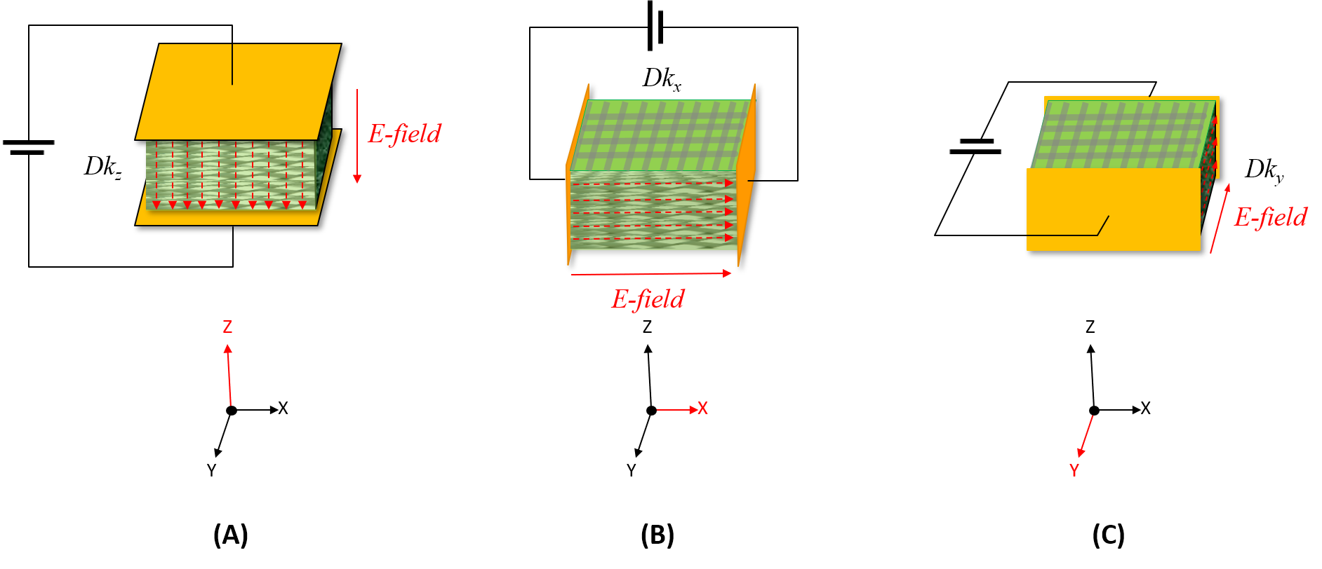
Figure 1. E-field orientation relative to the glass weave reinforcement in PCB laminates when a DC electrical potential is applied: E-fields are out-of-plane with respect to the glass weave (A) and in-plane with the glass weave (B, C).
Figure 1b and 1c show that when the conducting plates are placed perpendicular to the direction of the glass weave, the E-fields align with the x or y axis and are in-plane. Even though there might be slight variations in the effective Dk in these directions, heuristically we assume they are equal and refer to them as Dkxy.
Depending on the test method used, Dk measured may be different due to the test fixture’s generated E-field orientation relative to the glass weave. Figure 2 summarizes E-field orientation when compared against popular test methods used by CCL suppliers. Dk obtained by these test methods are denoted as in-plane (Dkxy) or out-of-plane (Dkz).
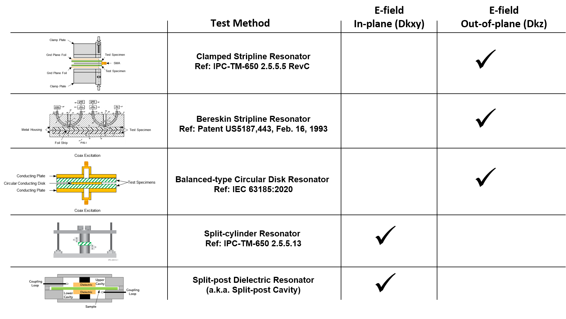
Figure 2. Comparative table of E-field orientation and resulting Dkxy or Dkz across popular test methods employed by CCL suppliers.
Dkxy is typically higher compared to Dkz, depending on the glass resin mixtures of the sample tested as shown in Figure 3a.

Figure 3. Rule of solid mixtures: Parallel mixing rule is used when E-fields are polarized in Z-direction (A) and series mixing rule is used when E-fields are polarized in x-y direction (B).
The rules of solid mixtures1 can be used to estimate anisotropy of the glass and resin mixture. If the E-field is polarized in the z-direction, using a Dk of 6.8 for E-glass (Dkg), a Dk of 2.5 for resin (Dkr), volume fraction of resin (vresin = 0.7), and volume fraction of E-glass (vglass = 0.3), then the effective capacitance of each block is in series and Dkz is determined to be 3.09, using the parallel mixing rule defined by:

When the conductor plates are moved, as shown in Figure 3b, and the mixture is polarized such that the E-field is parallel to the x-y axis, then the effective capacitance is in parallel and Dkxy is determined to be 3.79, using the series mixing rule defined by:

Using Equation 3, Anisotropy (Λ) of the mixture reveals that Dkxy is 23% higher than Dkz.

Anisotropy Implications for Via Modeling
PCB transmission lines run parallel to the glass weave and E-fields are predominantly out-of-plane. Thus, Dkz is needed for accurate impedance modeling. Using Dkxy instead means the impedance predicted from the field solver will be lower than what would be measured if the board was made exactly as specified in the stackup.
In the case of modeling vias, it gets more complicated. In Figure 4, given a cross-section view of a typical via and stub, we observe the E-fields as the signal propagates, from left to right, along the microstrip transmission line on the top layer, through the via to an inner stripline layer 3 and continuing through the stub.

Figure 4. Cross-section view of E-fields as a 20 GHz signal propagates from the microstrip top layer through a via with stub to a stripline layer 3 (HFSS simulation courtesy of Juliano Mologni, Ansys4).
Using the same value for Dk when modeling transmission lines and vias leads to inaccurate results for one or the other. If the CCL supplier’s published numbers are out-of-plane, Dkz, then the impedance for transmission lines will be correct, while the via impedance will end up being lower than modeled. On the other hand, if the published numbers are in-plane, Dkxy, then the via impedance will be correct and the transmission line impedance will end up being higher.
Furthermore, using the wrong Dk for modeling via stubs will result in poor simulation correlation to measurements2 and potentially the loss of channel margin due to maximum stub length guidelines based on simulation analysis.3 This can be problematic for 112/224 Gbps interconnects by reducing already tight margins.
Figure 5 shows an example of this issue. A 26 mil (0.66 mm) pitch differential via with a 10 mil (0.254 mm) stub model was created in Keysight ADS5 via designer (see Figure 5a). A Dkz of 3.09 and Dkxy of 3.79 from Equation 1 and Equation 2 were used in the model for comparisons. After finite element method (FEM) simulation, S-parameters were saved in touchstone format and simulated in the circuit schematic shown in Figure 5b.

Figure 5. Simulated results for differential IL/RL (C) and TDR impedance (D) of a differential via model with 10 mil (0.254 mm) stub using Dkz of 3.09 (red plots) and Dkxy of 3.79 (blue plots) for laminate. Modeled and simulated with Keysight ADS5 via designer.
Figure 5c compares differential insertion loss (IL) and return loss (RL) and Figure 5d compares differential time domain reflectometer (TDR) impedance. The red plots are using out-of-plane Dkz and the blue plots are using in-plane Dkxy. As can be seen, when out-of-plane Dkz value is used in the model, it underestimates IL and impedance by approximately 8 Ohm. For 112 Gbps, the difference in loss at 28 GHz Nyquist frequency is ~ 0.3 dB. At 56 GHz Nyquist for 224 Gbps, the delta is ~ 0.9 dB, caused by the difference in stub resonant nulls at 106 and 95 GHz.
But this doesn’t tell the whole story. While it is widely known that short, highly reflective channels can negatively impact channel performance, the issue has been exacerbated by the introduction of 4-level pulse amplitude modulated (PAM4) signaling, which reduces the signal-noise ratio by 9.5 dB. As bit rates continue to increase exponentially, traditional IL/RL masks and eye diagrams are no longer sufficient for assessing channel quality.
Channel operating margin (COM)7 is a system-level metric approach adopted by the IEEE 802.3ck standard to validate the performance of a serial link. As part of COM, there is an effective return loss (ERL) metric that factors in reflections caused by impedance mismatches at the pins of the transmitter, receiver, and any other discontinuities between them. Thus, COM can be used to assess the impact of Dk anisotropy on key metrics.
A short channel representing a typical chip-to-chip (C2C) topology was modeled by concatenating touchstone files for vias and transmission lines using Keysight ADS5, as depicted in Figure 6b. The 2 in. (5.08 cm), 100 Ohm differential transmission line was modeled with Polar SI90006 using an out-of-plane Dkz value of 3.09.

Figure 6. Simulated TDR and COM results when Dkz was used for vias and transmission lines compared to when Dkxy was used for via models and Dkz used for transmission lines. When Dkz was used for all models COM and ERL passed (d), but when Dkxy was used for the via models, COM passes with reduced margins and ERL failed (E).
Figure 6a shows the differential TDR response obtained using a Dkz value of 3.09 for the via and transmission line models. As shown in Figure 6d, both COM and ERL passed when a short package model was used. When the via files were replaced with files modeled with Dkxy of 3.79, the differential TDR response is degraded, as shown in Figure 6c. Figure 6e shows that although COM passed, it had reduced margins and ERL failed.
Of course, this was an extreme example with high Dk anisotropy. Choosing a dielectric with low Dk glass and higher resin content would improve the results. But if you have a tight loss budget to begin with, using the wrong numbers could cause failure to meet compliance once your board is built and tested.
Summary
Since woven glass PCB substrates are anisotropic, EDA design and modeling software hoping to advance AI and ML algorithms should have provisions to model anisotropic material, especially via transitions.
It is important to have awareness of the test method used by CCL suppliers for accurate modeling and simulation. Using out-of-plane Dkz values instead of in-plane Dkxy values for via modeling can cause misleading simulation results, which may result in reduced margins and potential compliance test failures when the design is built and tested.
It is recommended that CCL suppliers provide anisotropic properties in their Dk/Df construction tables. In lieu of that, my DesignCon 2024 paper and presentation titled “A Heuristic Approach to Assess Anisotropic Properties of Glass-reinforced PCB Substrates” will be delving deeper into anisotropy to reveal how to calculate anisotropy from CCL suppliers’ Dk/Df construction tables. The full paper will be made available following the event.
April 3, 2024 update: The DesignCon paper is now available on my web site:

REFERENCES
-
P. S. Neelakanta, “Handbook of Electromagnetic Materials: Monolithic and Composite Versions and Their Applications,” CRC Press LLC, 1995.
-
L. Simonovich, E. Bogatin, and Y. Cao, “Differential Via Modeling Methodology,” IEEE Transactions on Components, Packaging and Manufacturing Technology, Vol. 1, No. 5, pp. 722–730, May 2011, doi: 10.1109/TCPMT.2010.2103313.
-
B. Simonovich, “Via Stubs – Are They all Bad?”, Signal Integrity Journal, March 10, 2017
-
ANSYS, Inc. Headquarters, Southpointe, 2600 Ansys Drive, Canonsburg, Pa., 15317, U.S.
-
Keysight PathWave Advanced Design System (ADS) [computer software], (Version 2023, Update 2).
-
Polar Instruments Si9000 [computer software], (Version 22.09.01).
-
IEEE802.3ck COM v3.70, computer software.
Book Review: BOGATIN’S PRACTICAL GUIDE to TRANSMISSION LINE DESIGN and CHARACTERIZATION for SIGNAL INTEGRITY APPLICATIONS
Originally published Signal Integrity Journal March 20, 2023
 I often get asked by young engineers what it takes to become a good SI/PI or EMC engineer. I quickly respond with, “What’s on your bookshelf?”, because I’m a firm believer you can never learn too much on a particular subject. So answering the same question about myself, I would say, “A lot of books by Dr. Eric Bogatin”.
You might ask, “Why so many of his books?”. The reason is Eric always has something new to teach me. Especially with one of his latest books, “BOGATIN’S PRACTICAL GUIDE to TRANSMISSION LINE DESIGN and CHARACTERIZATION for SIGNAL INTEGRITY APPLICATIONS”. The 603 page book is available in two formats, e-book and hard cover print. Both versions are available through Artech House.
I started with the e-book version, but later got the hard cover book because I’m old school and like to have hard copy books on my book shelf as a quick reference. If you are trying to decide which version to buy, I recommend the e-book. You see, Eric has trailblazed the industry, once again, with this version. If you have been following Eric’s teachings through his webinars and videos, you would now have the best of both worlds on your hard drive.
In the first chapter, Eric asks the question, “Do we really need another transmission line book?”, then goes onto explain his reason why we do. I would however, ask another question, “Do we really need a Different transmission line book?”.
Here’s why:
The e-book is multimedia. Eric has cleverly integrated video tutorials to reinforce the written text to further cement his teachings. By clicking on embedded hyperlinks to a secure web sight, you get to watch a short video related topic. It is like having Eric as your own personal virtual tutor you can watch over and over to strengthen the concepts he has described in the text.
The internet is full of content dealing with transmission lines. Much of the content you read is full of complex math equations and confusing explanations that is often been copied and filtered from other blog sights and articles for marketing click-bait. Some of it is just plain wrong or misinterpreted by the author. This just leads to more fear, uncertainty and doubt; a.k.a. FUD.
Instead, Eric Bogatin’s book starts with basic fundamentals of transmission lines explained and filled with practical examples and videos. At the end of each chapter there are review questions and the answers are found in the Appendix. By the end of the book, you will come away with the understanding of;
-
lossless vs lossy transmission lines
-
the difference between instantaneous impedance; input impedance; odd/even mode impedance; and characteristic impedance
-
microstrip vs stripline geometry and what are the first and second order effects on impedance
-
single-ended vs differential transmission lines
-
reflections when instantaneous impedance changes
-
terminating transmission line circuits
-
the physics of crosstalk and mitigation techniques
-
return and displacement currents and their roles in transmission lines
-
what every scope user needs to know about transmission lines
-
and more……
Furthermore, Eric also blends in actual practical time domain reflectometry (TDR) measurement experiments as well as SPICE circuit models with open sourced Quite Universal Circuit Simulator (QUCS) software. He provides links to the software and most importantly, he provides the actual QUCS circuit files he used in his video tutorials so you can play around with them yourself. This greatly accelerates your learning curve.
As a signal integrity practitioner, I’m used to thinking and analysing transmission lines in the time domain. One of the things I finally understood by reading the book is how to analyze transmission lines in the frequency domain. That’s when I experienced the ah-ha moment and realized that I could simply determine the characteristic impedance of a transmission line if I followed the 2-port shunt VNA measurement technique, popular in the PI world.
I’m sure you can scour the internet and search for similar content, but why would you want to, when everything you practically wanted to know about transmission lines, you can get in one reference book. It has something for everyone, whether a young engineer starting out, or seasoned grey-hairs, like me. I wished I had this book 25 years ago when I began my journey with signal integrity.
So to answer Eric’s original question, “Do we really need another transmission line book?” Well, after reading the book, I would confidently say, “Yes!”
Field Solver Nuances: How to avoid GIGO
To avoid “garbage in, garbage out” (GIGO) with any field solver, first you need to understand the little nuances of PCB fabrication process and how to interpret manufacturers’ data sheets. But most importantly you need to understand the tool’s user interface and what it is asking for.
All 2D or 3D field solvers will give accurate impedance predictions. The differences are the type of solvers used under the hood and complexity of the user interface. Simple 2D field solvers, used in many of today’s stackup planners, simply give predicted characteristic impedance based on material properties and trace geometries. More complex, 2.5D or 3D field solvers, allow for additional material parameters and can predict insertion loss, phase delay and impedance over frequency. Some will even export RLGC and touchstone files for further signal integrity analysis.
Standard PCBs are fabricated using cores and prepreg material. Prepreg sheets are a mixture of fiberglass (glass) cloth and resin which is partially cured. Cores are simply cured prepreg sheets with copper bonded to one or both sides of the laminate. Copper is etched away on each side of the foil to leave the circuit pattern.
In a multi-layer PCB, cores and prepreg sheets are alternately stacked symmetrically above and below the middle of the layup then pressed under heat and pressure. The prepreg layers gets thinner when pressed allowing the resin to fill the voids between the copper features that were etched away on the cores.
One important parameter for accurate impedance modeling is dielectric constant (Dk). The best source is from laminate suppliers’ data sheets. But all data sheets from laminate suppliers are not the same.
“Marketing” data sheets are data sheets easily found on laminate suppliers’ websites. They are meant for quick comparison of dielectric properties to narrow your search for the right laminate for your application. They include mostly thermal and mechanical properties, which are important for the physical structure of the material and how it will perform with other material properties in the stackup during processing [3].
Marketing data sheets usually only report a typical Dk value at fifty percent resin content at two or three frequency points. Depending on glass style, resin content and thickness, Dk and dissipation factor (Df), will be different for different cores and prepreg thicknesses for the same laminate chemistry. In the end, they are not representative of what is needed to design an actual stackup, or to do impedance and loss modeling. Using these numbers will almost always lead to inaccurate impedance and signal integrity (SI) results.
Instead, you need to use the same Dk/Df construction table data sheets PCB fabricators use for the stackup. Dk/Df construction tables provide the actual core and prepreg thicknesses, resin content, and Dk/Df for the different glass styles, over different frequencies. Depending on the stackup, a combination of thicknesses is often needed to meet impedance requirements and have different Dk values.
Many engineers assume Dk published is the intrinsic property of the material. But in fact, it is the effective Dk (Dkeff) measured by a specific industry standard test method. It does not guarantee the values directly correspond to design applications. When compared against measurements from a design application, there is often a discrepancy in Dkeff due to increased phase delay caused by surface roughness [1].
Dkeff is highly dependent on the test apparatus and conditions of how it is measured. One popular test method, IPC-TM-650 2.5.5.5C clamped stripline resonator test method, assures consistency of product during fabrication. Due to the nature of this test method, the materials under test are not physically bonded together, air is entrapped between the various layers. These small air gaps are caused by: roughness of the copper foil plates in the fixture; roughness profile imprint left on the surface from the foil that was removed from the test samples; copper removed on the resonant element pattern card. Air entrapment results in a lower Dkeff than what is measured because in a real PCB everything is bonded together, with no air entrapment [3].
All glass weave reinforced laminates are anisotropic, which means E-field orientation, relative to the glass weave, is different depending on test method. E-fields produced from tests like IPC-TM-650 2.5.5.5C are transverse to the glass weave and Dkeff measured is out-of-plane.
E-fields produced by TM-650-2.5.5.13 split post cavity resonators, are parallel to the fiberglass weave Dkeff measured this way is in-plane. Dkeff is typically higher for in-plane measurements, compared to out-of-plane, depending on the glass resin mixtures used in the stackup.
Another source of discrepancy is not accounting for increased Dkeff due to the pressed thickness of prepreg. Since prepreg sheets have a certain percentage of resin content for the thickness, after pressing the resin content is reduced and since Dk is a function of resin and glass mixture, there will be a higher percentage of glass after pressing and thus slightly higher Dkeff.
The most common PCB trace geometries are micro-strip and stripline. A simple microstriip geometry is bare copper traces over a reference plane, separated by a dielectric height H, as shown in Figure 1. Depending on the stackup, there may be a core and prepreg layer between the outer layer and reference plane with the same or different Dk values for Dk1 and Dk2.
Simple stripline geometry has copper traces between two reference planes. For single-ended (SE) signals, there is only one trace used in the field solver to calculate the SE impedance. For differential pairs, there are two traces separated by a space. Because resin fills the voids between copper features the Dkresin will be lower than Dk1 or Dk2, shown in Figure 1.
The last thing to note is the wider side of the trace always faces the core material. This is a very important point to remember when using any field solver. If you get it reversed, it will lead to inaccurate results.

Figure 1 Generic microstrip and stripline geometries.
Thickness of copper traces is an important parameter for accurate impedance prediction. Copper thickness is usually specified in ounces per square foot. Most common thicknesses for inner layer traces are ½ oz. and 1 oz. foil. But field solvers expect an actual thickness dimension.
Most designers assume 0.7 mils (18um) thickness and 1.4 mils (36um) for ½ oz. and 1 oz. respectively. But because of the price of copper, the copper you get from foil manufacturers will likely be the minimum thickness allowed under IPC-4562A. When you factor in the typical thickness after fabrication, the typical thickness can be 0.6 mils (15um) and 1.2 mils (30um). But the minimum thickness allowed under IPC-A-600G-3.2.4 is 0.45 mils (11.4um) and 0.98 mils (24.9 um) for ½ oz. and 1 oz. respectively.
Due to the nature of the etching process, the traces will usually be trapezoidal in shape. This is known as the etch factor (EF), as defined by IPC-A-600G. It is the ratio of the thickness (t) to half the difference between W1 and W2.
Thus,
![]()
Some field solvers will define EF differently so it is important to understand how to specify it properly.
Once you’ve come up with a proposed stackup, the next step is to do some impedance modeling. Normally your fab shop comes up with this, but it is a good idea to validate their proposal, to ensure you are in sync with them.
The first thing to do, is identify the layers from which to model. Next, is to use your field solver, to model characteristic impedance. Since all field solvers are different, and user interfaces can be confusing, make sure you understand the little nuances of your tool.
The next thing is to identify the core layers in the stackup and input H1 and Dk1 for the dielectric. Then, input the pressed thickness for prepreg H2 and Dk2, not the thickness found in Dk/Df construction tables. You can usually trust the pressed thickness from your fab shop. But be careful how the field solver defines H2. Most field solvers define it as shown in Figure 1, but some solvers, like Polar Si9000e, define it as (H2+t), shown in Figure 2. Usually, you can trust the pressed thickness from your board shop stackup drawing.
Finally, if your field solver allows for it, fill in Dkresin between two traces if you know it. It will be lower than Dk2. Since this number is generally hard to obtain, a rough estimate to use is the lowest Dk value from the highest resin content prepreg found in Dk/Df construction tables.
Once everything is set up, optimize the line width and space, until the desired characteristic impedance is reached. One last point to remember, is that all 2D field solvers only calculate lossless characteristic impedance. But when we measure an impedance test coupon with a time domain reflectometer (TDR), we are measuring the instantaneous impedance along the PCB trace.
More often than not, impedance is different than what was predicted. This is because a 2D field solver only calculates the lossless characteristic impedance of the cross-sectional geometry; while a TDR measures the instantaneous impedance of a lossy transmission line at every point along its length.
A 2D field solver has no input for conductor resistivity, dielectric loss, or how long the conductor is. Resistive loss often results in a slow monotonic rise in the impedance profile. IPC-TM-650 specifies the measurement zone between 30-70 % and most PCB fab shops, will measure an average impedance
In this example, shown in Figure 2, for a low loss dielectric, there is a 4-5 ohm difference depending on where the measurement is taken. When all input parameters are included correctly for a lossy transmission line model, you can see there is excellent correlation.

Figure 2 Lossless characteristic impedance from Polar SI9000 field solver (left) vs measured TDR plot from an impedance coupon and lossy transmission line model from Polar Si9000.
Although minor differences in individual parameters may have second order affects, collectively they could add up to give poor correlation to measurements. But if you consider all the nuances discussed in this article, you can get pretty good accuracy as shown in Figure 2.
[1] Bert Simonovich, “A Practical Method to Model Effective Permittivity and Phase Delay Due to Conductor Surface Roughness”, DesignCon 2017, Santa Clara, CA
[2] Bert Simonovich, “PCB Fabrication: What SI/PI Engineers Need to Know for First Time Modeling Success”, DesignCon 2021 Spring Break Webinar, April 12, 2021
[3] Bert Simonovich, A Tale of Two Data Sheets and How Foil Roughness Affects Dk, White paper
A Tale of Two Data Sheets Part 2: Making Sense of “Design” Dk
Originally published in Signal Integrity Journal, May 31, 2022
In part one, “A Tale of Two Data Sheets”, I explained how air entrapment, due to IPC-TM-650-2.5.5.5 test method manual [7], is the primary reason for effective dielectric constant (Dkeff) and phase delay discrepancies between simulation and device under test (DUT) measurements. Entrapped air of the test fixture results in a lower Dk published in laminate suppliers’ Dk/Df tables than what would be measured in a real printed circuit board (PCB) application. This is because in a real PCB, everything is bonded together with no air entrapment, as shown in a cross-section view of Figure 1.

Figure 1. Example of foil bonded to core or prepreg dielectric. Rz is 10-point mean roughness of foil as measured by a profilometer. Hsmooth is the thickness of the dielectric as if the foil was removed.
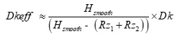
When copper foil with the same Rz roughness is bonded to each side of the core or prepeg, Dkeff is determined heuristically from published Dk by this simple correction factor [1]:
Equation 1.

where:
Hsmooth is the thickness of the dielectric as if the foil was removed
Dk = Dielectric constant published in laminate suppliers’ Dk/Df tables
Rz = 10-point mean equivalent to Rz(JIS) or Rz(DIN) published in foil suppliers’ data sheets. This is not to be confused with Rq, which is RMS value of roughness.
Rogers Corporation [4] understands this. That’s why they provide the “design” Dk in addition to their bulk Dk, as measured by TM650 clamped stripline resonator test method [7]. Design Dk is an average number using a differential phase length method from several different tested lots of material and on the most common thickness. This method is based on measuring phase difference from two identical microstrip transmission line geometries, of different lengths on the same panel. Because this is a real microstrip application, the dielectric is fully bonded to the copper and there is no air entrapment. Knowing the phase and length difference, the effective Dk is empirically determined.
The accuracy of the resultant effective Dk depends on several factors like:
-
-
fixture design
-
-
-
length ratio between two transmission lines
-
-
-
material thickness of the sample under test
-
-
-
the thickness of the copper
-
-
-
actual roughness of the foil on the microstrip circuit.
-
In lieu of actual Dk/Df tables, Rogers provides a handy impedance calculator as shown in in the RO4003C example of Figure 2. There are three Dk options available to use:
-
-
Z-axis bulk Dk
-
-
-
Dk values for specific frequencies
-
-
-
Dk values for characteristic impedance
-
The first radio button, as shown in Figure 2, gives the z-axis bulk Dk value of 3.55, as measured by TM650 2.5.5.5 test method manual. However, the value does not change when different frequencies are selected. This makes the number suspect since clearly design Dk does change over frequency. Thus this number can be considered equivalent to marketing data sheets, and should not be used.
When the middle radio button is selected, a Dk value for a specific frequency is displayed, which corresponds to a frequency entered in the lower right frequency box of Figure 2. This is the most useful option, since it allows the user to choose the right design Dk at whatever frequency they choose for their application, including characteristic impedance. This option already factors in the foil roughness effect, so no correction factor is needed to use in your simulator.
The last radio button selects a Dk for characteristic impedance calculation. It is a “design” Dk with yet a different Dk. Similar to the Bulk Dk option, it does not change over frequency. For any simulation tool other than the Rogers’s calculator, Bulk Dk and Dk values for characteristic impedance values should not be used.

Figure 2. Example of Rogers Corporation impedance calculator. For an 8-mil thick RO4003C dielectric, bulk Dk is 3.55 while design Dk over frequency is shown in bottom left window.
Under the information tab, the user can download design Dk over frequency, for a specified thickness, shown in the bottom left window of Figure 2. This data can be selected and copied to the clipboard and pasted into a spreadsheet for further processing.
Figure 3 plots design Dk vs. frequency for various thickness from 8 mils to 60 mils for RO4003C material. As can be seen, design Dk is not constant over frequency and furthermore it is different for different thicknesses, mainly due to the roughness of the foil that is already included in the measurement.
Thinner materials have a higher design Dk than thicker materials for the same roughness of foil. This is because when the foil teeth protrude into a thin dielectric material, there is a higher concentration of e-fields, resulting in higher capacitance between top and bottom copper layers. For thick dielectrics the foil teeth have less of an impact on capacitance and thus Dkeff, as described mathematically by Equation 1.
Since the roughness of the foil does not significantly influence the design Dk for thick laminates, we can assume the bulk Dk is roughly equivalent to design Dk over frequency for the 60-mil laminate.

Figure 3. Design Dk vs. frequency for various thickness of RO4003C from 8 mils to 60 mils mainly due to the roughness of the foil. Thinner material has a higher design Dk than thicker material, for the same roughness of foil.
Heuristically, we can rearrange Equation 1 and estimate the Rz roughness of the foil used on RO4003C laminate to be 6.302 μm from Equation 2.
Equation 2.

where:
Hsmooth is the thickness of the 8 mil (203 μm) laminate
DkBulk = 3.55 at 60 GHz for 60 mil (1524 μm) laminate
Dkeff = design Dk of 8 mil (203 μm) laminate at 60 GHz
A cross-section sample from a time domain reflectometry (TDR) demo board, courtesy of Picotest [6], was measured and is shown in Figure 4. The TDR demo board was fabricated with 8-mil thick Rogers RO4003C core laminate and cladded with 2 Oz copper foil.
Five highlighted random sample lengths of copper roughness, labeled Sample 1 to Sample 5 of Figure 4, were analyzed. The total length of each respective sample was then partitioned into five equal sections, similar to the blow-up picture of Sample 1, to measure the maximum peak to valley height of each section. The five measurements of each sample length were then averaged to determine the Rz roughness, as described under IPC TM650 2.2.17A [8] and shown in the table of Figure 4.
The mean value of Rz for the five samples was 6.176 μm with a standard deviation (SD) of 1.090 μm. This compares favorably with the estimated roughness of 6.302 μm, determined from Equation 2.

Figure 4. A cross-section sample from a Rogers RO4003C based TDR demo board, courtesy of Picotest [6], used to determine Rz roughness of the foil.
When we use the actual roughness measured from Figure 4 and Equation 1, we can then calculate Dkeff at 60 GHz for different thicknesses, shown in Table 1. As can be seen there is, less than 1% delta compared with design Dk reported from the calculator!
Table 1. Comparison of Roger’s Design Dk vs. Dkeff when simple correction factor applied to Bulk Dk at 60 GHz.
|
Height |
Height |
Bulk Dk |
Design Dk |
Rz |
Dkeff |
Delta |
|
8.0 |
203 |
3.550 |
3.785 |
6.176 |
3.780 |
-0.13% |
|
12.0 |
304 |
3.550 |
3.702 |
6.176 |
3.700 |
-0.04% |
|
16.0 |
406 |
3.550 |
3.657 |
6.176 |
3.661 |
0.12% |
|
20.0 |
508 |
3.550 |
3.625 |
6.176 |
3.638 |
0.37% |
|
32.0 |
812 |
3.550 |
3.580 |
6.176 |
3.605 |
0.69% |
|
60.0 |
1524 |
3.550 |
3.550 |
6.176 |
3.579 |
0.82% |
Rogers Corporation provides a handy calculator in lieu of Dk/Df tables in which “design” Dk values over frequency can be used directly without correcting for roughness. When an actual cross-section was analyzed, there was excellent correlation from corrected Dkeff using heuristic methods compared to design Dk from the calculator. Therefore, “design” Dk should be used for impedance modeling and PCB stackup design when using Rogers laminates.
References:
-
-
B. Simonovich, “A Tale of Two Data Sheets and What You Need to Know About Dielectric Constant (DK),” Signal Integrity Journal article, April 2022.
-
-
-
L. Simonovich, “A Practical Method to Model Effective Permittivity and Phase Delay Due to Conductor Surface Roughness,” DesignCon 2017, Santa Clara, USA.
-
-
-
Isola Group, 6565 West Frye, Chandler, AZ 85226.
-
-
-
Rogers Corporation, 2225 W. Chandler Blvd., Chandler, AZ 85224.
-
-
-
J. Coonrod, “Managing PCB Materials: Dielectric Constant (Dk)”, Rogers Corporation, Blog Article, Sep 11, 2018.
-
-
-
Picotest, Phoenix, AZ 85085.
-
-
-
IPC-TM-650, 2.2.17A, Test Methods Manual, “Surface Roughness and Profile of Metallic Foils (Contacting Stylus Technique).”
-
-
-
Bereskin, A. B. “Microwave Dielectric Property Measurements”, Microwave Journal, vol. 35, no.7, pp. 98 – 112.
-
A Tale of Two Data Sheets: Part1
Originally published SI Journal April 26, 2022
When doing printed circuit board (PCB) stackup and signal integrity (SI) impedance modeling, we need to get the dielectric material properties from the right sources. One important parameter for accurate impedance modeling is relative permittivity (εr) of the dielectric material, otherwise known as dielectric constant (Dk). The best source is from laminate suppliers’ data sheets. Though there is an issue with these I like to think of as, “a tale of two data sheets.”
Marketing data sheets, like the example shown in Figure 1 [6], are easily found on laminate suppliers’ websites. They are meant for quick comparison of dielectric properties to narrow your search for the right laminate for your application. Dielectric properties on marketing data sheets include mostly thermal and mechanical properties, which are important for the physical structure of the material and how it will perform with other material properties in the stackup during processing.
But marketing data sheets are not representative of what is needed to design an actual stackup, or to do impedance and SI loss modeling. Depending on glass style, resin content, thickness, Dk, and dissipation factor (Df) will be different for different cores and prepreg thicknesses for the same laminate. Marketing data sheets usually only report a typical Dk/Df at fifty percent resin content and two or three frequency points. Thickness is not specified. Furthermore, Dk and Df are not constant over frequency. So, using numbers from these data sheets will lead to inaccurate impedance and phase delay results.
Figure 1. Example of a “Marketing” data sheet easily obtained from laminate supplier’s web site. Source Isola Group [6].
Instead, for transmission line modeling, one needs to use the same Dk/Df table data sheets PCB fabricators use to build the stackup. An example Dk/Df table is shown in Figure 2. Dk/Df tables provide the actual core and prepreg thicknesses, resin content, and Dk/Df for the different glass styles, over different frequencies. Depending on the stackup, a combination of thicknesses is often needed to meet impedance requirements. Each thickness will have a different Dk value.
In the example of Figure 2, Dk varies from 2.92 at 10 GHz for 1080 glass style to 3.19 at 10 GHz for 2116 glass style. This represents a Dk variation of -3.3% to 5.6% when compared to a Dk of 3.02 at 10 GHz specified in Figure 1.
Figure 2. Example of a typical “Engineering” data sheet showing Dk/Df table for different glass styles and resin content over frequency. Source Isola Group [6].
Many engineers assume Dk published is the intrinsic property of the material. But, in fact, it is the effective Dk (Dkeff) measured by a specific industry standard test method. When they are compared against real measurements from a design application, there is often a discrepancy in Dkeff due to increased phase delay caused by surface roughness [1].
Dkeff is highly dependent on the test apparatus and conditions of how it is measured. One method commonly used by many laminate suppliers is the clamped stripline resonator test method, as described by IPC-TM-650 2.5.5.5, Rev C, Test Methods Manual [10].
Since all glass reinforced laminates are anisotropic, any stripline based test method, like TM-650 2.5.5.5, or Bereskin stripline test method [13], reports Dk values in which the E-fields are transverse to signal propagation. That is, if the signal propagation is in the x-y axis direction, then the Dk measured by this method is when E-fields are in the z-axis direction.
For Isola’s Dk/Df table [6], shown in Figure 2, Dk values were measured by TM-650 2.5.5.5 test method. From that data, the values for most of the constructions are calculated. Additional verification runs are performed to gather statistical data over time and validate that the calculations are reasonable and accurate.
The measurements are done under stripline conditions using a carefully designed resonant element pattern card. It is made with the same dielectric material to be tested. As shown in Figure 3, the card is sandwiched between two sheets of uncladded dielectric material under test. Then the whole structure is clamped between two large plates; each lined with copper foil and grounded. They act as reference planes for the stripline.
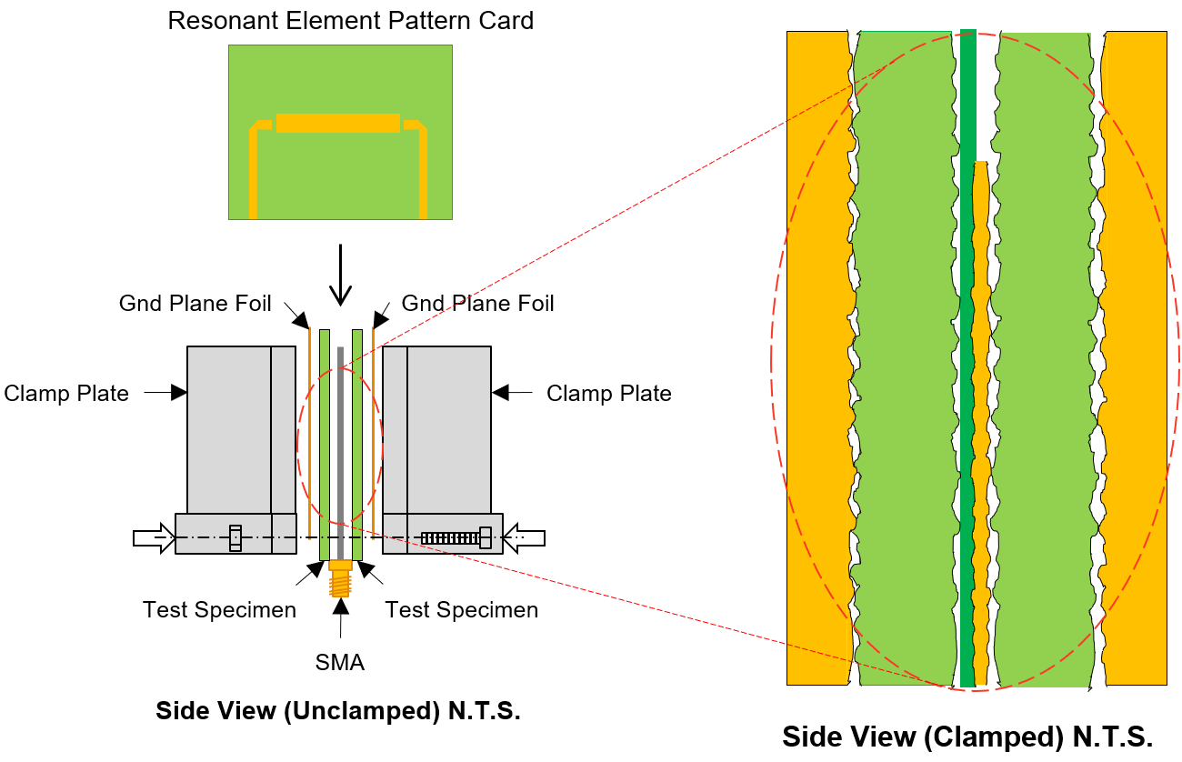
Figure 3. Illustration of clamped stripline resonator test method, as described by IPC-TM-650, 2.5.5.5, Rev C, Test Methods Manual [10].
This test method assures consistency of product when used in fabricated boards. It does not guarantee the values directly correspond to design applications.
Here is why:
Since the resonant element pattern card and material under test are not physically bonded together, air is entrapped between the various layers. These small air gaps are caused by the:
-
roughness of the copper foil plates in the fixture
-
roughness profile imprint left on the surface from the foil that was removed from the test samples
-
copper removed on the resonant element pattern card
Air entrapment, due to the TM-650 test method, is the primary reason for effective Dk and phase delay discrepancies between simulation using laminate suppliers’ Dk/Df tables and real measurements from a design application. The small air gaps result in a lower effective Dk than what would be measured in a real PCB because everything is pressed together with no air entrapment, as shown in a cross-section view of Figure 4.

Figure 4. Example of foil bonded to core or prepreg dielectric. Rz1 is rougher than Rz2 and Hsmooth is the thickness of the dielectric as if the foil was removed.
When copper roughness is different on each side of the dielectric, like the example shown in Figure 4, Dkeff is determined heuristically by this simple correction factor:
Equation 1.
where:
-
Hsmooth is dielectric core thickness from laminate suppliers’ Dk/Df table data sheet or pressed prepreg thickness from the PCB stackup drawing.
-
Rz1 and Rz2 are the conductor roughness of the foil for the respective side of the dielectric from foil suppliers’ data sheet. Typically, Rz is the 10-point mean roughness as measured by a mechanical profilometer.
-
Dk is dielectric constant from laminate supplier’s Dk/Df table data sheet.
In Figure 4, Rz1 is the roughness of the top foil, and Rz2 is the roughness of the bottom foil. In this example, Rz1 is rougher than Rz2. Hsmooth is the core thickness of the dielectric, as specified in the Dk/Df table, or pressed thickness of the prepreg, often shown on a stackup drawing. It is the thickness of the dielectric as if the foil was removed.
When copper foil with the same Rz roughness is bonded to each side of the core or prepeg, Dkeff can be simplified as:
Equation 2
Figure 5 plots Dkeff over frequency derived from S21 phase or time delay (TD); Dkeff=(TDc0 ∕ length)2 from a Megtron-6 stripline case study [3]. This method is different than IPC-TM-650 test method in that it determines Dkeff from unwrapped phase delay rather than calculating Dk/Df from resonant peaks over the frequency range defined in the spec.
The blue plot is a simulated case based on core and prepreg Dk values from published Dk/Df tables at 12 GHz. When Dk is corrected due to roughness, using Equation 2, and resimulated, Dkeff is shown in pink. Although the Dkeff has improved, it still does not agree with the measured Dkeff from the device under test (DUT), shown in red.
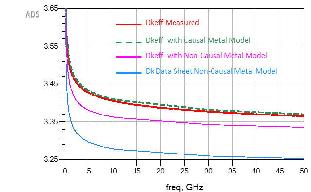
Figure 5. Comparisons of simulated Dkeff over frequency vs. measured. The red plot is actual measured Dkeff from the DUT. The middle pink plot is a simulation using Dkeff corrected due to roughness. The bottom blue plot is simulated using Dk at 12 GHz as published in Dk/Df tables and non-causal roughness model. The green dashed plot is a simulation using Dkeff due to roughness; a causal Huray-Bracken roughness model was used. Modeled with Simbeor [11] and simulated with Keysight ADS [12].
The discrepancy between the pink and red plots is because Dkeff from Equation 2 only corrects the phase delay due to self capacitance (C11) per unit length of the transmission line. But roughness of the foil also increases the self inductance (L11) per unit length of the transmission line, which adds additional phase or time delay [4].
This is counter intuitive and can be confusing since we usually relate Dkeff to capacitance only. By definition, Dkeff is the ratio of the actual structure’s capacitance to the capacitance when the dielectric is replaced by air. But this is only true for static electric fields. For time-variant electromagnetic fields, Dkeff becomes frequency-dependent [14].
If the propagation delay (tpd) for a single transmission line, in seconds per unit length, is determined by:
Equation 3.
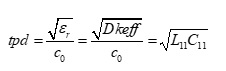
and c0 is the speed of light (~3.0E8 m/s) =1/sqrt(μ0 ε0 ); μ0 (4πE−7 H/m) and ε0 (8.8542E−12 F/m) is permeability and permittivity of free space respectively, then:
Equation 4.
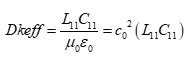
where: L11; C11 are self inductance in Henries per unit length and self capacitance in Farads per unit length respectively.
Equation 4 clearly shows that with an increase in self inductance there will be a proportional increase in Dkeff. This means for PCB transmission lines, calculating Dkeff=(TDc0 ∕ length)2 cannot be trusted to be the same as relative permittivity (εr) of the dielectric material. The consequence for doing so leads to inaccurate impedance predictions and non-causal time domain simulations, resulting in poor correlation to measurements.
A causal model, when simulated, does not produce any change in its output signal before there is a change in its input signal. When field solvers properly correct the self inductance, by applying the roughness correction factor to the imaginary portion of the complex impedance of the metal [4][5], the model is then causal. When combined with the corrected Dkeff for cores and prepregs from Equation 2, there is excellent correlation, as shown by the dashed green plot in Figure 5. Unfortunately, not all field solvers have causal roughness models to correct the inductance in the simulation.
Since there is no simple way to backtrack from a phase measurement to establish the right Dkeff to use for your modeling, especially for lossy stripline constructions, heuristic methods are an alternative.
Using the right Dkeff for your modeling ensures a correct time domain reflectometer (TDR) impedance prediction, as shown in Figure 6. The red plot is measured differential TDR from [3]. When core and prepreg Dk from Dk/Df tables were used along with a non-causal roughness model in the simulation, the blue plot shows an overestimate for impedance. When Dkeff from Equation 2, and a non-causal roughness model was used in the simulation, the pink plot shows an underestimate in the impedance plot.
It is only when we apply a causal Huray-Bracken roughness model from [11], along with Dkeff from Equation 2, that we see the effect of the increased self inductance, shown by the green dashed line plot in Figure 6.
At first glance of Figure 6, one might interpret the pink plot as having better correlation to the measured red plot. But because the measured plot has an impedance ripple along its length, it is difficult to conclude which is the correct model from the TDR plots alone. It is only when we compare Dkeff derived from the green dashed phase delay plot from Figure 5 that we can conclude the green dashed line TDR plot is the correct impedance.
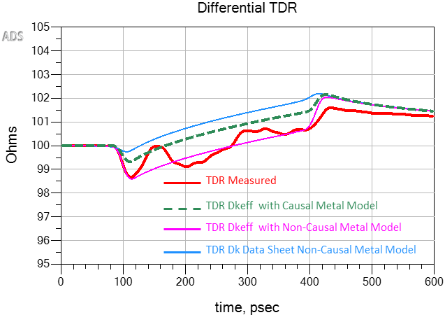
Figure 6. Simulated vs. measured differential TDR plots when different Dkeff was used in the model. The blue plot overestimates impedance when Dk from data sheets was used. The pink plot underestimates the impedance when Dkeff (Equation 2) and non-causal roughness model was used. The green dashed line plot is when Dkeff (Equation 2) and a causal Huray-Bracken roughness model were used. Modeled with Simbeor [11] and simulated with Keysight ADS [12].
Summary:
Dielectric constants from marketing data sheets cannot be trusted to properly design PCB stackups and model transmission lines for impedance and phase delay. Instead, laminate suppliers’ Dk/Df tables should be used.
Many laminate suppliers provide Dk/Df tables derived from a clamped stripline resonator test method [10] or similar Bereskin test method [13]. But the numbers do not factor the actual roughness of the foil. When a simple correction factor, based on the thickness of laminate and Rz foil roughness is considered, a more accurate value for Dkeff along with a causal roughness model can be used for impedance and transmission line modeling.
For PCB transmission lines, calculating Dkeff from phase or time delay measurement method cannot be trusted to be the relative permittivity of the dielectric material. Using this value will lead to inaccurate simulation results.
References:
1. L. Simonovich, “A Practical Method to Model Effective Permittivity and Phase Delay Due to Conductor Surface Roughness“, DesignCon 2017, Santa Clara, USA.
2. B. Simonovich, “Stackup Beware: Case Study of the Effects on Transmission Line Losses Due to Mixed Reference Plane Roughness”, Signal Integrity Journal article, August 10, 2021.
3. B. Simonovich, “PCB Fabrication: What SI/PI Engineers Need to Know for First Time Modeling Success”, DesignCon 2021 Spring Break Webinar Series, April 12-16, 2021.
4. V. Dmitriev-Zdorov, B. Simonovich, Igor Kochikov, “A Causal Conductor Roughness Model and its Effect on Transmission Line Characteristics“, DesignCon 2018, Santa Clara, USA.
5. J.E. Bracken, “A Causal Huray Model for Surface Roughness”, DesignCon 2012, Santa Clara, USA.
6. Isola Group, 6565 West Frye, Chandler, AZ 85226.
7. Circuit Foil, 6 Salzbaach, 9559 Wiltz, Grand Duchy of Luxembourg.
8. Rogers Corporation, 2225 W. Chandler Blvd., Chandler, AZ 85224.
9. J. Coonrod, “Managing PCB Materials: Dielectric Constant (Dk)”, Rogers Corporation, Blog Article, Sep 11, 2018
10. IPC-TM-650, 2.5.5.5, Rev C, Test Methods Manual
11. Simbeor THz [computer software].
12. Keysight ADS Keysight Advanced Design System (ADS) [computer software].
13. Bereskin, A. B. “Microwave Dielectric Property Measurements”, Microwave Journal, vol. 35, no.7, pp. 98 – 112
14. Wikipedia contributors. (2022, January 12). Relative permittivity. In Wikipedia, The Free Encyclopedia. Retrieved 18:14, January 14, 2022.
The Effects on Transmission Line Losses Due to Mixed Reference Plane Roughness Case Study
This article is an edited version of White Paper, “Heuristic Modeling of Transmission Lines due to Mixed Reference Plane Foil Roughness in Printed Circuit Board Stackups” [1].
Designing the right printed circuit board (PCB) stackup can make or break your product performance. If your product has circuitry that is transmission loss sensitive, then paying attention to conductor surface roughness is paramount.
Conductor surface roughness traditionally has been applied to copper foil to promote adhesion to the dielectric material. Early PCBs were only constructed with single or double-sided copper core laminates. The only important metric for copper was its purity and the roughness to improve peel strength. There was no such thing as a PCB stackup and nobody worried about impedance or transmission line losses.
But over the years PCBs have evolved into multi-layer constructions with evermore attention being paid to impedance control and transmission line losses. Thus a PCB stackup definition became vital for consistent performance.
Like any construction project, you need a blueprint before you start building. Similarly for PCBs, you need a stackup drawing and detailed fabrication notes. Part of the stackup design process includes signal integrity (SI) modeling for characteristic impedance and transmission loss. If your design is running at 56Gig pulse amplitude modulation level 4 (PAM-4), for example, you are probably looking at low loss dielectrics and low roughness copper for the signal traces.
But what is sometimes overlooked in the stackup, is the roughness of the reference planes. Often thin core laminate power and ground (GND) planes will specify reverse-treated foils (RTF), which are rougher on the side that bonds to the prepreg. Sometimes one of these planes, usually GND, acts as a reference plane to an adjacent signal layer as shown in Figure 1. If that adjacent high-speed signal layer is using smoother copper than one or both reference planes, a higher insertion loss than expected for that layer will occur and possibly ruin your day.
A similar scenario could occur for high density interconnect (HDI) technology. This is a popular method to increase component density on modern PCBs. By the nature of their stackup construction, a rougher copper reference plane could sometimes also end up adjacent to a signal layer as well. Thus, if insertion loss is a concern, copper foil roughness of reference planes needs to be considered.

Figure 1 An example cross-section stripline geometry from a stackup showing thin core laminate (top) with RTF bonded to prepreg and adjacent to a high-speed differential pair with smooth foil.
So how do you know this before you design your stackup and build your first prototype? Since we do not have any empirical data to go by, we can rely on a heuristic, high-level design (HLD) modeling method starting with published parameters found solely in manufacturer’s data sheets.
Heuristic HLD modeling is a practical technique that is not guaranteed to be perfect, but is still adequate in finding a satisfactory solution sooner, rather than later.
For dielectric parameters, we choose dielectric constant (Dk) / dissipation factor (Df) at or near the Nyquist frequency of the baud rate, then apply effective Dk (Dkeff) correction factor due to roughness, Equation 1 [5].

where:
H = thickness of core/prepreg; Rz is surface roughness of copper; Dk is as published in laminate supplier’s Dk/Df tables. Equation 1 assumes Rz of the foil on each side of the dielectric (core or prepreg) is the same.
For conductor loss, we use Rz roughness numbers from copper suppliers’ data sheets and oxide/oxide alternative Rz roughness numbers from your favorite fab shop, then apply the Cannonball-Huray roughness model [1]-[3].
Cannonball-Huray Model
The original Huray model is defined as:
Equation 2

The Cannonball-Huray model allows you to extract the right parameters using Rz roughness for core and prepreg sides of the foil [1]. Because the Cannonball-Huray model assumes the ratio of Amatte/Aflat = 1, and Ni = 14 spheres, the radius of a sphere (r) can be determined by:
![]()
and area of flat tile base (Aflat) by:
Equation 4

Wildriver Isola I-Tera® MT40 Custom Modeling Platform Case Study
To study the effect of reference plane roughness on transmission insertion loss, Wildriver Technology’s [7] custom modeling platform (CMP), shown in Figure 2, was used as a case study. This CMP was custom developed for Isola [6] to characterize their new I-Tera® MT40 very low-loss laminate material.
It combines 27 structures based on a consistent development of primitive structures; useful for performing a host of calibrations including automatic fixture removal, unknown THRU, WinCal XE™ calibration, and VNA gating and time transform analysis.

Figure 2 Wildriver Isola I-Tera® MT40 Custom Modeling Platform. Source: Wildriver Technology [7]
Stackup Validation
The PCB stackup is shown in Figure 3. Often PCB fab shop field application engineers (FAE) modify existing stackups and unintentionally make errors in transferring new parameters from data sheets into their software tools. Also, they may not necessarily know the design intent of the stackup. So the first step for any model correlation exercise is to sanitize the stackup, to ensure it meets the product design intent for signal integrity (SI) performance. In fact that is how the issue of different plane roughness was uncovered.
Since it is always a good practice to ensure the same roughness is specified for reference planes as the adjacent signal layers, I naively assumed it would be the case for any high-speed stackup. But that wasn’t the case here. Layers E1,E2 and E7, E8 specify 1oz RTF, while layers E3, E4 and E5, E6 specify 1oz VLP2 foil. Because the Isola I-Tera® MT40 CMP is intended to aid in modeling test structures, this is not a fatal flaw. On the contrary, it is a perfect platform to assess the effect of rougher reference planes.

Figure 3 Isola I-Tera® MT40 Custom Modeling Platform stackup. Source: Wildriver Technology [7]
Upon further review, it was discovered that the core laminates between E3,E4 and E5, E6 specified 1067/2×3313 glass styles, but this combination was not listed for 12 mil thickness. Instead, only 3×3313 core is offered. Because of that, the Dk shown is also wrong and will affect the impedance of the traces. The right Dk for 3×3313 is 3.53 instead if 3.33.
Foil Roughness
As mentioned earlier, the roughness of the foil affects the effective Dk, so we need to use the right number for our model validation. The standard VLP2 foil, used on I-Tera® MT40 core laminates is BF-TZA foil. Optional RTF foil, used for layers E1, E2 and E7, E8, is TWLS-B. Both are from Circuit Foil [8].
Relevant roughness parameters are shown in Figure 4. For the core side of the foil we are interested in the Rz parameters for the treated side listed in the table. But there are two Rz parameters, JIS B 601 and ISO 4287 specified. So which one do we use for modeling?
From IPC-TM-650 Section 1.2 [11] states, “The foil profile of foils shall be evaluated using the parameter Rz (DIN) or RTM, which is defined as the average maximum peak to valley height of five consecutive sampling lengths within the measurement length. This value is approximately equivalent to the values of profile determined from microsectioning techniques.”
and;
Section 1.3 states, “RZ (ISO) is a different parameter from Rz (DIN) and is not applicable to this method.”
Rz JIS represents the 10-point mean value, which is the sum of the average of the 5 highest peaks and the 5 lowest valleys over the sample length. Rz DIN is similar; except it is defined as the average maximum peak to valley height of five consecutive sampling lengths within the measurement length. Thus we will use Rz JIS for modeling analysis.

Figure 4 Roughness parameters from Circuit Foil [8] data sheets. Top is VLP2 standard foil used on I-Tera® MT40, while bottom is RTF option used for relevant layers in the stackup
Determine Effective Dk Due to Roughness
The first step in HLD impedance modeling is to gather all the dielectric and foil data sheet parameters to determine the effective Dk.
Figure 5 summarizes thickness of core, prepreg and signal trace from the stackup geometry in Figure 3. Note that photos are for illustrative purposes only and are not actual cross-sections from CMP PCB. Dk for core and prepreg were obtained from Isola I-Tera® MT40 Dk/Df tables [6].

Figure 5 Data sheet parameters for RTF/VLP2 foil roughness and dielectric properties for I-Tera® MT40 stackup geometry. Note: Photos are for illustrative purposes only and are not actual cross-sections from CMP PCB. Surface roughness pictures source: Circuit Foil [8]
The top reference plane is TWLS-B RTF foil with matte side 1 ≤ 7.5 JIS, obtained from Circuit Foil data sheet (Figure 4). The roughness surface profile is shown in the upper left. After OA smoothing, 1 ≤ 6.23 [1].
BF-TZA foil is used for both sides of the core laminate. The top surface of the stripline trace, shown in the upper right picture, is the drum side of the foil, before OA treatment. After OA treatment, Rz2 ~ 1.9 μm [1].
The bottom surface profile of the stripline trace and the top surface of the bottom reference plane are the treated matte sides of the foil, shown in the bottom right and bottom left pictures respectively. They both share the same roughness (Rz3, Rz4 =2.5μm JIS) from the BF-TZA data sheet (Figure 4).
The next step is to convert the imperial thickness units to metric, then use Equation 1 to determine Dkeff due to roughness for the prepreg and core.

Determine Cannonball-Huray Roughness Parameters
Several popular electronic design automation (EDA) tools include the Cannonball-Huray model directly as an option, so the respective Rz parameter is all that is needed.
Any of these tools can be used for HLD modeling, but my favorite is Polar SI9000 [9] because of its simplicity and sufficient accuracy for prefabrication modeling and analysis. Many fab shops use this tool for impedance prediction, so it is easy to stay in sync with them during the HLD stage of your project. Plus, it has the added benefit of modeling transmission loss and exporting S-parameters in touchstone format for further channel modeling in other tools.
Because Polar Si9000 assumes all the reference planes have the same roughness, it only allows Rz roughness parameters to be inputted for the matte and drum side of the signal trace. The best we can do, is take the average roughness of Rz1,Rz2 and Rz3,Rz4:

Simulation Correlation
When Dkeff due to roughness values were used instead of published Dk values, the new impedance prediction is 48.24 ohms, as shown in Figure 6.

Figure 6 Polar Si9000 impedance prediction with Dkeff due to roughness
Dkeff/Df for H1, H2 was then inputted into the causal dielectric model at 10GHz, as shown in Figure 7 (left), while Rzmatte, Rzdrum was inputted into the Cannonball-Huray model (right).

Figure 7 Causal Dkeff/Df dielectric and Cannonball-Huray roughness model input panels in Polar Si9000
After a 6-inch transmission line was simulated, the S-parameters were exported in touchstone format. Keysight Pathwave ADS [10] was used for further processing and analysis.
Figure 6 compares simulated insertion loss vs de-embedded reflectionless generalized modal (GM) S-parameter measurements, provided by Wildriver Technology [7]. As you can see there is excellent correlation without fitting to measured data!

Figure 8 HLD Insertion Loss simulation correlation for as designed stackup from data sheet and stackup parameters
Figure 9 plots simulated Dkeff vs measurements. At 10 GHz, simulated Dkeff is 0.105 (-2.8%) lower than measured value. Without actual cross-section microscopic measurements, it is difficult to conclude if the published Dk is wrong, or if there is process variation with roughness parameters used in the model.
But it is also interesting to note that measured Dkeff is not a constant value over frequency, as shown in the I-Tera® MT-40 Dk/Df tables. Instead Figure 9 reveals it varies over frequency, so the Dk/Df data sheet numbers are suspect.
Regardless, for the HLD modeling process, the simulation results are within acceptable tolerance.

Figure 9 HLD Dkeff simulation correlation for as designed stackup
Exploring the Effects of Alternate Foil Roughness
Now that we have good correlation to measurements, we can repeat the HLD modeling process to explore different foil roughness options. Figure 10 summarizes the thickness of core, prepreg and signal trace for VLP2/VLP2 foil (top) and VLP1/VLP1 foil (bottom). Note that photos are for illustrative purposes only and are not actual cross-sections from CMP PCB.
Respective Dkeff, and Cannonball-Huray roughness parameters were recalculated with same steps as VLP2/RTF case above.

Figure 10 Alternate foil options simulated for what-if loss comparison. Top is VLP2/VLP2 foil parameters for all copper layers and bottom is VLP1/VLP1 foil parameters for all copper layers. Note: Photos are for illustrative purposes only and are not actual cross-section from CMP PCB. Surface roughness pictures source: Circuit Foil [8]
Figure 11 presents the simulation results of all three scenarios. As expected. when the reference plane foil roughness went from RTF/VLP2 to VLP2/VLP2 there was improvement. At 14 GHz it was 0.5 dB and at 28GHz it was 1 dB improvement.
When VLP1/VLP1 foil was used, it was further improved by 0.8 dB and 1.7 dB at 14 GHz and 28 GHz respectively. So if your design is loss sensitive, you might want to consider VLP1 foil option.
When we compare Dkeff plots, we see effective Dk approaches actual Dk/Df data sheet values in the tables when smoother copper is used, as expected [5].
Since Dkeff was derived by phase delay, propagation delay will be affected by rougher copper.

Figure 11 What-if simulation comparison of VLP2/RTF, VLP2/VLP2, VLP1/VLP1 foil options and their effect on insertion loss and Dkeff
Conclusions
1. Roughness of reference planes make a significant difference in loss and phase delay, especially if one of the reference planes is RTF. If loss is important then all high-speed reference planes should have the same foil roughness specified
2. Heuristic HLD modeling method is a useful and accurate way to determine prefabrication impedance and loss predictions using data sheet parameters.
3. Published Dk from I-Tera® MT40 Dk/Df data sheet tables is not a flat constant over frequency.
4. Confirmed Rz JIS is the right parameter to use from Circuit Foil data sheet, instead of Rz ISO.
Acknowledgements
· Al Neves, CTO Wildriver Technology, for providing the custom modeling platform design details and measured data for the case study.
· Michael Gay, Director Business Development – Strategic Accounts at Isola Group, for providing foil supplier’s data sheets used on I-Tera® MT40 laminates.
References
[1] B. Simonovich, “Heuristic Modeling of Transmission Lines due to Mixed Reference Plane Foil Roughness in Printed Circuit Board Stackups”, White Paper, Lamsim Enterprises Inc.
[2] B. Simonovich, “Practical Method for Modeling Conductor Surface Roughness Using The Cannonball Stack Principle”, White Paper, Lamsim Enterprises Inc.
[3] L. Simonovich, “Practical method for modeling conductor roughness using cubic close-packing of equal spheres,” 2016 IEEE International Symposium on Electromagnetic Compatibility (EMC), 2016, pp. 917-920, doi: 10.1109/ISEMC.2016.7571773.
[4] L. Simonovich, “PCB Interconnect Modeling Demystified”, DesignCon 2019, Proceedings, Santa Clara, CA, 2019
[5] B. Simonovich, “A Practical Method to Model Effective Permittivity and Phase Delay Due to Conductor Surface Roughness”. DesignCon 2017, Proceedings, Santa Clara, CA, 2017
[6] Isola Group S.a.r.l., 3100 West Ray Road, Suite 301, Chandler, AZ 85226, URL: http://www.isola-group.com/
[7] Wild River Technology LLC 8311SW Charlotte Drive Beaverton, OR 97007, URL: https://wildrivertech.com/
[8] Circuit Foil 6 Salzbaach, 9559 Wiltz, Grand Duchy of Luxembourg URL: https://www.circuitfoil.com/portfolio/
[9] Polar Instruments Si9000e [computer software] Version 2018, URL: https://www.polarinstruments.com/index.html
[10] Keysight Pathwave Advanced Design System (ADS) [computer software], (Version 2021 update2). URL:http://www.keysight.com/en/pc-1297113/advanced-design-system-ads?cc=US&lc=eng.
[11] IPC-TM-650 Test Methods Manual 2.2.17A, Surface Roughness and Profile of Metallic Foils (Contacting Stylus Technique), 2/2001 Rev. A
[12] IPC-TM-650, 2.5.5.5, Rev C, Test Methods Manual
Characteristic Impedance – Where SI/PI Worlds Collide
Originally published Signal Integrity Journal, February 23, 2021
Signal and power integrity (SI/PI) simulations, measurements, and analysis usually live in two different worlds, but occasionally these worlds collide. One such collision occurs when we refer to characteristic impedance, Z0. Traditionally the PI world lives in the frequency domain while the SI world lives in the time domain.
When designing a power distribution network (PDN) in the PI world, we are mostly interested in engineering a flat impedance below a target impedance from DC to the highest frequency components of the transient current. Practically this is achieved with a network of capacitors with different values connected to the respective power planes as shown in Figure 1.

Figure 1 A simplified model of a typical PDN courtesy [1].
In the real world, there is no such thing as an ideal capacitor. There are always parasitic elements known as equivalent series inductance (ESL) and equivalent series resistance (ESR). Physical characteristics of the PCB, like component mounting inductance, plane spreading inductance, via and BGA ball inductance, along with voltage regulator module (VRM) characteristics also contribute to the impedance profile. When connected together, the interaction of capacitors and parasitic inductance and resistance create a transfer impedance profile with resonant peaks and anti-resonant nulls as shown in Figure 2.
The transfer impedance between the VRM and the load is calculated and plotted in the frequency domain with a log-log scale. The resulted impedance curve is then compared to the target impedance (Ztarget), which is estimated based on the allowed noise ripple and maximum transient current. The flat target impedance is frequency independent in the analysis.

Figure 2 Impedance profile of the PDN as viewed from the pads on the die power rail courtesy [1].
Resonant peaks are due to ESL of one capacitor connected in parallel with another capacitor. Anti-resonant nulls are due to the series combination of ESR, ESL, and C for each capacitor. Different capacitor values will have anti-resonant nulls at different frequencies.
But in the PI world, there is a rarely talked about characteristic impedance, Z0. In this case, it refers to the geometric average of the reactive impedance of a capacitor (XC) and reactive impedance of an inductor (XL).
Equation 1

At resonance, XL and XC intersect at the characteristic impedance and are equal as shown in Figure 3.

Figure 3 Inductive and capacitive reactance plot of ideal inductor and capacitor versus frequency. At resonance, XL and XC are equal and intersect at the characteristic impedance, Z0. Simulated with Pathwave ADS [6].
This is a very important observation, and it is where the SI/PI worlds collide.
In the SI world, characteristic impedance, Z0 refers to the instantaneous ratio of the voltage to current of a wave front traveling along a uniform transmission line without reflections. For an infinitely long uniform transmission line, Z0 equals the input impedance.
The characteristic impedance of a lossy transmission line is defined as:
Equation 2

Where R is resistance per unit length; G is conductance per unit length; L is inductance per unit length; and C is capacitance per unit length. For a lossless uniform transmission line, R and G are assumed to be zero and thus the characteristic impedance is reduced to:
Equation 3

Time Domain Reflectometer
In the SI world, we usually use a time domain reflectometer (TDR) to measure characteristic impedance, but more often than not, the measured impedance we get is not what we predicted with a 2D field solver. Many 2D field solvers used by most PCB FAB shops only calculate the lossless characteristic impedance of the cross-sectional geometry at a single frequency, defined by the dielectric constant (Dk). It has no input for conductor resistivity, dielectric loss, or how long the conductor(s) is.
So the issue is: we design the stackup, then do our SI modeling analysis based on stackup parameters and matching characteristic impedance. But the PCB FAB shop will often adjust the line width(s), over and above normal process variation, so that when measured, the impedance will fall within the specified tolerance, usually +/-10 percent.
Part of the problem lies with the method used to take the measurements. Most PCB FAB shops follow IPC-TM-650 Test Methods Manual [2]. But it has limitations because Z0 measured is derived and cannot be directly measured. The reason is the measurements include resistive and dielectric losses, up to the point where the measurement takes place along the TDR plot.
Resistive loss often results in a slow monotonic rise in the impedance profile, shown in the example TDR plot of Figure 4. IPC-TM-650 specifies a measurement zone between 30-70 percent to avoid probing induced ringing affecting the measurements. Most PCB FAB shops will measure an average impedance over this range, usually in the center region.
Depending on the linewidth, thickness and dielectric dissipation factor (Df), the slope of the monotonic rise will vary.

Figure 4 Example TDR plot showing slow monotonic rise in impedance due to resistive losses and IPC-TM-650 measurement zone.
The problem is that the IPC-TM-650 test method was last updated back in 2004, when higher dielectric loss, along with wider line widths and thicker copper weights, were used more often. A higher Df tends to compensate for resistive loss by flattening the slope as shown in Figure 5.
On the bottom left is a simulated TDR plot using a high loss dielectric with Df = 0.024. The right side has the exact same geometry properties except Df = 0.004. The average impedance, when measured at the 50 percent point, is 49.8 Ohms on the left side vs. 51.4 Ohms on the right side. We also confirm flatter slope for high loss material.
The actual characteristic impedance predicted by a Polar SI9000 2D field solver [5] in Figure 5 is 49 Ohms. For higher loss material, measuring within the measurement zone would pass without any issues. But for lower loss material, the resistive loss dominates and measuring within the measurement zone will give ~5 percent higher impedance reading compared to the higher loss material. The correct measurement point for Z0 is, in fact, the initial dip, equivalent to the field solver prediction. Depending on the tolerance specified, this may affect yield and cost.

Figure 5 Characteristic impedance prediction by Polar SI9000 2D field solver [5] (top). Simulated 2 inch TDR plots using a high loss dielectric (bottom left) vs. low loss dielectric with exactly the same geometry (bottm right). A higher Df compensates for higher resistive loss thereby flattening the curve. Simulated with Pathwave ADS [6].
Today, with the push to low loss dielectric and finer line widths with thinner copper weights, measuring the true transmission line characteristic impedance using a TDR becomes more challenging. This is even more so when measuring differential impedance, because a change in line width space geometry can have a more profound effect on measured differential impedance.
Using the first article build of a new design, as an example, let’s assume the correct characteristic impedance, when measured at the beginning of the slow monotonic rise of a TDR plot, is on the high end of nominal +10 percent tolerance. Let’s say it’s 54 Ohms. But because of the low loss dielectric and high resistive loss, the TDR measurement at the midpoint is now reading 5% higher at 57 Ohms. This would imply the impedance is now out of spec over nominal and the board would be scrapped.
The PCB fab shop will then go back and adjust the linewidth accordingly for the next build to bring the measurement within range to their measurement set up. Doing this effectively lowers the true nominal characteristic impedance!
If subsequent manufacturing variations pushes the measured impedance within the measurement zone on the low end of the -10 percent tolerance, say 44 Ohms, then the true characteristic impedance, if measured at the initial dip, will be 5 percent lower at 42 Ohms and be out of spec. But the board will pass because it was measured following IPC-TM-650 test method.
2-port Shunt Measurement
But what if there were another way? What if we could borrow impedance measuring techniques from the PI world to determine the true transmission line characteristic impedance in the SI world? Well there is. Enter the 2-port shunt measurement technique.
For example, in the PI world, to measure ESL and ESR of a chip capacitor, of a device under test (DUT), a 2-port shunt measurement is often used. It is much like the 4-point Kelvin measurement technique used to measure very low DC resistance.
The 2-port shunt measurement is usually done with a 2-port vector network analyzer (VNA). Port 1 of the VNA sends out a calibrated signal, and port 2 measures the voltage signal across the DUT. Often an isolation transformer is also used to break the inherent ground loop when measuring ultra-low impedances [3].
Once the measurements have been completed and S-parameters saved in touchstone format, further analysis can be done in your favorite SPICE simulator. Figure 6 is a generic schematic using popular Pathwave ADS [5] that can be used for 2-port shunt analysis.
When port 1 and port 2 are connected to port 1 of the DUT and port 2 of the DUT is grounded, the impedance of the DUT can be determined by [3];
Equation 4


Figure 6 Generic Pathwave ADS [6] schematic used for 2-port shunt analysis on a S2P file for DUT.
If we replace the DUT in Figure 6 with a capacitor and inductor, we get an impedance plot shown in Figure 7. As we saw earlier, when we take the geometric average of the inductive and capacitive reactance using Equation 1, we get the characteristic impedance. If we apply Equation 4 to the results of a 2-port shunt measurements of a capacitor and inductor, we get exactly the same results as shown in the top of Figure 7.
When we replace the capacitor and inductor with a S-parameter file of a transmission line model from Figure 5, we get the plot shown at the bottom of Figure 7. Except for the resonant nulls and peaks, up to a certain frequency, the impedance of a transmission line looks like the impedance of a capacitor when the far-end is open, and looks like the impedance of an inductor when the far-end is shorted. And because of that, this is where the two worlds collide!
If we take the geometric average of the impedance when the far-end is open (Zopen) or shorted (Zshort), we get the characteristic impedance at that frequency. We note where the red and blue impedance lines first intersect, is exactly the geometric average characteristic impedance at that frequency.
Also worth noting, the lines intersect at half of the frequency between the peaks and valleys at higher frequencies as well.

Figure 7 Impedance of inductive and capacitive reactance vs. frequency (top) and impedance of a transmission line vs. frequency (bottom) when the far-end is open (solid red) compared to when the far-end is shorted (solid blue). The intersection of the red and blue lines is exactly the characteristic impedance. Simulated with Pathwave ADS [5].
We can see this more clearly if we replot Figure 7 bottom using a linear scale for the x-axis, as shown in Figure 8. This is a very powerful observation. What this means is that when we measure the impedance half way between a peak and adjacent valley, of either the red or blue plot, it is the characteristic impedance of the transmission line at that frequency.
Thus, only an open or shorted end measurement is all that is needed to determine the characteristic impedance. For example, if we look at the red curve alone, then measure the first resonant null (m14) and adjacent peak (m15), the characteristic impedance (mag(Zopen) is measured exactly at one half the frequency between the two (m16).

Figure 8 Impedance of a transmission line vs. frequency on a linear scale when the far-end is open (solid red) compared to when the far-end is shorted (solid blue). The intersection of the red and blue lines half way between respective peaks and valleys is the characteristic impedance. Simulated with Pathwave ADS [6].
The first resonant red null and blue peak represent the quarter-wave resonant frequency due to open and shorted end. Each respective red null and blue peak following are the odd harmonics of the first quarter-wave resonant frequency.
Knowing this, we can now determine the phase or time delay (TD) of the transmission line as being one quarter of the period of the resonant frequency (f0).
Equation 5

Because resonant nulls and peaks occur at the resonant frequency, we can also determine the effective dielectric constant (Dkeff). Given the speed of light (c) = 11.8 in. per nanosecond, the length of the transmission line (len) in in. and quarter-wave resonant frequency (f0), Dkeff can be determined by:
Equation 6

CMP28 Case Study

Figure 9 Photo of a portion of CMP-28 test platform courtesy of Wildriver Technology [8] used for measurement validation.
To test the accuracy of this method, measured data from a CMP28 test platform, shown in Figure 9, was used for measurement validation. S-parameter (s2p) files from 2 inch and 8 inch single-ended stripline traces were provided as part of CMP-28 design kit courtesy of Wildriver Technologies [8]. The 6-inch transmission line segment S-parameter data was de-embedded courtesy of AtaiTec Corporation [9].
The characteristic impedance, based on trace geometry and stackup parameters, was modeled in Polar SI9000 [5]. Using Dk from data sheet tables @ 10GHz, and correcting for conductor roughness [10], the characteristic impedance predicted was 49.66 Ohms, as shown in Figure 10.

Figure 10 Polar SI9000 field-solver [5] characteristic impedance prediction of CMP28 trace geometry.
Touchstone S-parameter DUT files were connected with far-end open, shorted, and terminated as shown in Figure 11. The TDR plot, with far-end terminated, shows an impedance of 50.57 Ohms, when measured at the initial peak. Then it takes an immediate dip to approximately 50 Ohms before continuing with a slow monotonic rise with some ripples. If the DUT was a uniform trace, with connector discontinuity de-embedded, we would not see the initial peak followed by the dip. This signature strongly suggests that the DUT is not uniform and thus it is very difficult to determine the actual characteristic impedance using IPC-TM-650 test method alone.
But only after taking 2-port shunt measurements can we confirm the true characteristic impedance. As shown, Zoavg is 50.68 Ohms where the red and blue curves cross at 122.5 MHz, and confirms the true measurement point in the TDR plot is the initial peak. Both are about 1 Ohm higher compared with 2-D field solver results in Figure 10.
If the length of the transmission line simulated above is 6 in. and f0 =248.2 MHz, then TD = 1 ns and Dkeff = 3.92, using Equation 5 and Equation 6 respectively.

Figure 11 Measured results from a CMP28 test platform design kit, courtesy of Wildriver Technology [8].
But wait a minute. Why is Dkeff is higher than what was used in the 2-D field solver in Figure 10?
One reason is due to process variation of the material and fabrication. The actual Dkeff is determined by the final thickness of dielectric and the roughness of the copper, which also increases inductance affecting TD [10] [11]. But the main reason is Dk is frequency dependent and the value used in the field solver was at 10 GHz, based on laminate supplier’s Dk/Df tables.
Since TD, ultimately determines Dkeff, it does not represent the intrinsic property of the dielectric material. Because Dkeff varies with frequency, it was calculated at the first resonant null of 248.2 MHz, which is at a much lower frequency for Dk than the frequency originally used to select Dk in the field solver.
As can be seen in Figure 12, a simulated vs. measured 2-port shunt frequency plot, with far-end open and shorted, we get exactly the same information, compared to the traditional method used to validate characteristic impedance and Dkeff.
If we measure the 39th odd harmonic frequency (H) at 9.884GHz for the resonant null closest to 10GHz, equating to the value of Dk used in Polar Si9000 2D field solver, Dkeff can be calculated with Equation 7:
Equation 7

The bottom right plot of Figure 12, shows Dkeff simulated (blue) vs. measured (red). As we can see, the measured Dkeff at 248.7 MHz is 3.94; pretty much agreeing with our earlier calculation of 3.92 using Equation 6. Furthermore, when we compare Dkeff = 3.76 at 9.884 GHz, it agrees with our calculation for the 39th harmonic frequency from Equation 7. The reason there is still a slight difference in Dkeff is because the added delay due to inductance due to roughness [11] was not factored into the simulated model.
The bottom left is a TDR plot that shows measured impedance (red) vs. simulated (blue) over time. The marker at the beginning of the initial dip (m6) represents the characteristic impedance with highest frequency harmonics included in the incident step edge of TDR waveform. The marker at the end (m16) represents the impedance at twice the TD with high frequency harmonics attenuated due to dispersion of the lossy dielectric and resistance of trace length.
When we measure Zoavg_meas impedance of DUT at 9.884GHz, at the top plot of Figure 12, it agrees pretty well with the simulated and measured TDR plot at the initial step.

Figure 12 Comparison of PI world 2-port shunt measurement results for transmission line characteristic impedance and Dkeff compared to traditional SI world measurement results. Top plot is the 2-port shunt simulated vs. DUT impedance measurements at the fundamental and 39th harmonic frequencies. Bottom left is beginning and end impedance measurements on TDR plot. Bottom right measuring equivalent Dkeff at fundamental and 39th harmonic frequencies.
Summary and Conclusion
Sometimes, when SI and PI worlds collide, we get the best of both worlds. By borrowing a simple 2-port shunt impedance measuring technique from the PI world, we have another tool at our disposal to measure true characteristic impedance, TD, and effective Dk from a uniformly designed transmission line in the SI world. The advantage is, unlike a TDR measurement, measuring true characteristic impedance using 2-port shunt method is not influenced by resistive or dielectric losses.
References
-
L. Smith, S. Sandler, E. Bogatin, “Target Impedance Is Not Enough,” Signal Integrity Journal, Vol. 1, Issue 1, January 2019; URL: https://www.signalintegrityjournal.com/ext/resources/MEDIA-KIT-2019/January-2019-Print-Issue/SIJ-January-2019-Issue_eBook_-V2.pdf
-
IPC-TM-650 Test methods Manual, Number 2.5.5.7, “Characteristic Impedance of Lines on Printed Boards by TDR”, Rev. A, March, 2004
-
I. Novak, J. Millar, “Frequency-Domain Characterization of Power Distribution Networks,” Artech House, 685 Canton St., Norwood, MA, 02062, 2007.
-
Pathwave Advanced Design System (ADS) [computer software], Version 2021, URL: http://www.keysight.com/en/pc-1297113/advanced-design-system-ads?nid=-34346.0&cc=CA&lc=eng
-
Polar Instruments Si9000e [computer software], Version 2018, URL: https://www.polarinstruments.com/index.html
-
Keysight Pathwave Advanced Design System (ADS) [computer software], Version 2021, URL: http://www.keysight.com/en/pc-1297113/advanced-design-system-ads?cc=US&lc=eng.
-
E. Bogatin, “Bogatin’s Practical Guide to Transmission Line Design and Characterization for Signal Integrity”, Artech House, 685 Canton St., Norwood, MA, 02062, 2020
-
Wild River Technology LLC 8311 SW Charlotte Drive Beaverton, OR 97007. URL: https://wildrivertech.com/
-
AtaiTec Corporation, URL: http://ataitec.com/products/isd/
-
B. Simonovich, “A Practical Method to Model Effective Permittivity and Phase Delay Due to Conductor Surface Roughness“, DesignCon 2017 proceedings, Santa Clara CA.
-
V. Dmitriev-Zdorov, B. Simonovich, I. Kochikov, “A Causal Conductor Roughness Model and its Effect on Transmission Line Characteristics”, DesignCon 2018 proceedings, Santa Clara, CA.
-
I. Novak et al, “Determining PCB Trace Impedance by TDR: Challenges and Possible Solutions”, DesignCon 2013 proceedings, Santa Clara, CA.
-
S. Sandler, “Easy trick to measure plane impedance with VNA”, EDN Asia, 2014, URL: https://archive.ednasia.com/www.ednasia.com/STATIC/PDF/201410/EDNAOL_2014OCT21_TEST_TA_01.pdf%3FSOURCES=DOWNLOAD
Single-ended to Mixed-Mode Conversions
Originally published in Signal Integrity Journal Magazine, July 2020
Signal Integrity (SI) engineers almost always have to work with S-parameters. If you haven’t had to work with them yet, then chances are you will sometime in your SI career. As speed moves up in the double-digit GB/s regime, many industry standards are moving to serial link-based architectures and are using frequency domain compliance limits based on S-parameter measurements.
A vector network analyzer (VNA) is the test instrument of choice to measure S-parameters from a device under test (DUT). By definition, each S-parameter (Sij) is the ratio of the sine wave voltage coming out of a port to the sine wave voltage that was going in to a port (Equation 1). Each S-parameter is complex with a magnitude and a phase.

Suffice it to say, for mathematical reasons, the indexes refer to the port in which the voltages are coming or going. This is counter intuitive to our normal train of thought and is important to be cognisant of this relationship when working with S-parameters.
Single-ended S-parameters
Figure 1 shows an example of a 1-Port, 2-Port and 4-Port DUTs and their respective S-parameter matrices representing uniform transmission lines with respective port index labelling. Each S-parameter in the matrix are single-ended measurements from one port to another.
A 1-Port DUT has one S-parameter (S11) shown in red. It is the ratio of the voltage coming out of Port 1 to the voltage going into Port 1. As a measure of reflected energy out of Port 1, it is also known as return loss (RL)
A 2-Port DUT has 4 S-parameters shown in blue. S-parameters with the same index subscript numbers, i.e. S11, S22 are RL. S-parameters with alternate index subscript numbers, are a measure of transmitted energy and is the ratio of the voltage coming out of a Port to the voltage going into the opposite Port. It is also known as insertion loss (IL). For example, S12 is the ratio of the voltage coming out of Port 1 to the voltage going into Port 2, whereas S21 is the ratio of the voltage coming out of Port 2 to the voltage going into Port 1.

Figure 1 From left to right examples of 1-Port (Red), 2-Port (Blue), 4-Port (Black) DUTs and their respective S-parameter matrices.
A 4-Port DUT has 16 S-parameters, divided into 4 quadrants, shown in black. As you can see the number of S-parameter combinations is the square of the number of ports. In this example, the top left quadrant 1 and bottom right quadrant 4 are the same as individual 2-Port DUTs with different port indices. They are described as:
Quadrant 1:
-
S11 is the ratio of the voltage coming out of Port 1 to the voltage going into Port 1. It is the RL out of Port 1.
-
S12 is the IL and is the ratio of the voltage coming out of Port 1 to the voltage going into Port 2. It is the IL from Port 2 to Port 1.
-
S21 is the ratio of the voltage coming out of Port 2 to the voltage going into Port 1. It is the IL from Port 1 to Port 2. For a uniform transmission line, S21 = S12.
-
S22 is the ratio of the voltage coming out of Port 2 to the voltage going into Port 2. It is the RL out of Port 2. For a uniform transmission line, S22 = S11.
Quadrant 4:
-
S33 is the ratio of the voltage coming out of Port 3 to the voltage going into Port 3. It is the RL out of Port 3
-
S34 is the ratio of the voltage coming out of Port 3 to the voltage going into Port 4. It is the IL from Port 4 to Port 3
-
S43 is the ratio of the voltage coming out of Port 4 to the voltage going into Port 3. It is the IL from Port 3 to Port 4. For a uniform transmission line, S43 = S34.
-
S44 is the ratio of the voltage coming out of Port 4 to the voltage going into Port 4. It is the RL out of Port 4. For a uniform transmission line, S44 = S33
S-parameters in the top right quadrant 2 and bottom left quadrant 3 describe the near-end and far-end coupling of the respective ports. When unwanted coupling happens at the near-end, it is referred to as near-end cross talk, or NEXT. When it happens at the far-end, it is known as far-end crosstalk, or FEXT.
Quadrant 2:
-
S13 is the ratio of the voltage coming out of Port 1 to the voltage going into Port 3. It is the coupling or NEXT from Port 3 to Port 1.
-
S14 is the ratio of the voltage coming out of Port 1 to the voltage going into Port 4. It is coupling or FEXT from Port 4 to Port 1.
-
S23 is the ratio of the voltage coming out of Port 2 to the voltage going into Port 3. It is coupling or FEXT from Port 3 to Port 2.
-
S24 is the ratio of the voltage coming out of Port 2 to the voltage going into Port 4. It is coupling or NEXT from Port 4 to Port 2.
Quadrant 3:
-
S31 is the ratio of the voltage coming out of Port 3 to the voltage going into Port 1. It is the coupling or NEXT from Port 1 to Port 3.
-
S32 is the ratio of the voltage coming out of Port 3 to the voltage going into Port 2. It is coupling or FEXT from Port 2 to Port 3.
-
S41 is the ratio of the voltage coming out of Port 4 to the voltage going into Port 1. It is coupling or FEXT from Port 1 to Port 4.
-
S42 is the ratio of the voltage coming out of Port 4 to the voltage going into Port 2. It is coupling or NEXT from Port 2 to Port 4.
Although there is no industry standard for labeling a 4 or more port DUT, a practical way is to use the port order shown so that the 2-Port DUT is a subset of the top left quadrant of the 4-Port DUT. When you do this, the port order labeling is consistent as you increase the number of ports; with odd ports on the left and even ports on the right. S12 and S21 always describe the IL terms; while S13 and S31 define the NEXT terms.
But sometimes 3rd party 4-port S-parameters are labeled with ports 1 and 2 are on the left side, while ports 3 and 4 are on the right side. In this configuration, S31 and S42 are now the IL terms. This is counter intuitive when moving from 2-Port to 4 or more Port DUT and leading to potential confusion when cascading S-parameters to build a channel model, or converting to mixed-mode S-parameters. Whenever you get S-parameter files from 3rd party, it is always prudent to test it and compare IL plots against port order to ensure you are using them correctly.
Typically, 4-port S-parameters are saved in Touchstone format with a .snp extension, where n is the number of ports. Many Electronic Design Automation (EDA) and circuit simulation software tools allows you to view and plot S-parameters from Touchstone files.
Figure 2 is a schematic of a 4-port S-parameter component used in Keysight ADS. When the component is linked to appropriate .s4p touchstone file and ports connected as shown, the 16-port S-parameter matrix can be plotted and analyzed.

Figure 2 Keysight ADS schematic used to plot 4-Port single-ended S-parameters.
The 1-port and 2-port S-parameters are included in the same plot as the 4-port S-parameters plotted in Figure 3. The top left (red) and bottom right (green) quadrants plot the return loss (RL) and insertion loss (IL), while the top right (blue) and bottom left (magenta) quadrants plot the NEXT and FEXT.

Figure 3 An example of 4-Port S-parameter single-ended plots of a uniform transmission line.
Mixed-mode S-parameters
SI engineers often have to check channel models and S-parameter measurements against industry standard compliance plots. Many of those plots are in terms of mixed-mode S-parameters, which means the single-ended measurements need to be converted to mixed-mode matrix.
Two single-ended transmission lines with coupling are also known as a differential pair, as shown in Figure 4. When we talk about single-ended transmission lines with coupling, we are usually interested in their single-ended properties like characteristic impedance (Zo), phase delay, and NEXT/FEXT relationships as described above.
But when we talk about a differential pair, we are interested in the mixed-mode S-parameters like differential and common signals and how they interact within the pair. Because we are describing the exact same interconnect, they are equivalent.
When describing a differential pair, there are only four possible outcomes in response to an input signal as defined by the mixed-mode S-parameter matrix:
-
A differential signal enters the differential pair and a differential signal comes out
-
A differential signal enters the differential pair and a common signal comes out
-
A common signal enters the differential pair and a differential signal comes out
-
A common signal enters the differential pair and a common signal comes out

Figure 4 Single-ended vs mixed-mode S-parameter matrices of two coupled transmission lines.
Mixed-mode S-parameters in each quadrant are described as:
SDD Quadrant (Red):
-
SDD11 is the ratio of the differential signal coming out of Port 1 to the differential signal going into Port 1. It is the differential RL out of Port 1.
-
SDD12 is the ratio of the differential signal coming out of Port 1 to the differential signal going into Port 2. It is the differential IL from Port 2 to Port 1.
-
SDD21 is the ratio of the differential signal coming out of Port 2 to the differential signal going into Port 1. It is the differential IL from Port 1 to Port 2.
-
SDD22 is the ratio of the differential signal coming out of Port 2 to the differential signal going into Port 2. It is the differential RL out of Port 2.
SDC Quadrant (Blue):
-
SDC11 is the ratio of the differential signal coming out of Port 1 to the common signal going into Port 1.
-
SDC12 is the ratio of the differential signal coming out of Port 1 to the common signal going into Port 2.
-
SDC21 is the ratio of the differential signal coming out of Port 2 to the common signal going into Port 1.
-
SDC22 is the ratio of the differential signal coming out of Port 2 to the common signal going into Port 2.
SCD Quadrant (Magenta):
-
SCD11 is the ratio of the common signal coming out of Port 1 to the differential signal going into Port 1.
-
SCD12 is the ratio of the common signal coming out of Port 1 to the differential signal going into Port 2.
-
SCD21 is the ratio of the common signal coming out of Port 2 to the differential signal going into Port 1.
-
SCD22 is the ratio of the common signal coming out of Port 2 to the differential signal going into Port 2.
SCC Quadrant (Green):
-
SCC11 is the ratio of the common signal coming out of Port 1 to the common signal going into Port 1.
-
SCC12 is the ratio of the common signal coming out of Port 1 to the common signal going into Port 2.
-
SCC21 is the ratio of the common signal coming out of Port 2 to the common signal going into Port 1.
-
SCC22 is the ratio of the common signal coming out of Port 2 to the common signal going into Port 2.
Single-ended S-parameters, with port order shown in Figure 4, can be mathematically converted into mixed-mode S-parameters using equations shown in Table 1.

Alternatively, Keysight ADS can simplify this process using equations on 4-Port single-ended or using 4-port Balun components, as shown in Figure 5.

Figure 5 Keysight ADS schematic used to convert from 4-Port single-ended to 2-Port mixed-mode S-parameters using equations or 4-Port Balun components. Differential and common port numbering as D1, D2, C1, C2 respectively.
Figure 6 plots mixed-mode S-parameters from equations in Table 1. Each quadrant is color coded to coincide with the respective table quadrants.

Figure 6 An example of 4-Port S-parameter mixed-mode plots of a differential transmission line.
References:
[1] M. Resso, E. Bogatin, “Signal Integrity Characterization Techniques”, International Engineering Consortium, 300 West Adams Street, Suite 1210, Chicago, Illinois 60606-5114, USA, ISBN: 978-1-931695-93-0
https://www.amazon.com/Signal-Integrity-Characterization-Techniques-Bogatin-ebook/dp/B07P9277WY/ref=sr_1_fkmr0_1?keywords=bogaitn+resso&qid=1581289220&sr=8-1-fkmr0
[2] A. Huynh, M. Karlsson, S. Gong (2010). Mixed-Mode S-Parameters and Conversion Techniques, Advanced Microwave Circuits and Systems, Vitaliy Zhurbenko (Ed.), ISBN: 978-953-307-087-2,InTech, Available from: http://www.intechopen.com/books/advanced-microwave-circuits-and-systems/mixed-mode-s-parameters-and-conversion-techniques.
[3] Alfred P. Neves, Mike Resso, and Chun-Ting Wang Lee, “S-parameters: Signal Integrity Analysis in the Blink of an Eye”, Signal Integrity Journal, https://www.signalintegrityjournal.com/articles/432-s-parameters-signal-integrity-analysis-in-the-blink-of-an-eye
Keysight Advanced Design System (ADS) [computer software], (Version 2020). URL: http://www.keysight.com/en/pc-1297113/advanced-design-system-ads?cc=US&lc=eng.
