Archive for March 2011
The Poor Man’s PCB Via Modeling Methodology
You are a backplane designer and have been assigned to engineer a new high-speed, multi-gigabit serial link architecture from several line cards to multiple fabric switch cards across a backplane. These links must operate at 6GB/s day one and be 10GB/s (IEEE 802.3KR) ready for product evolution. The schedule is tight, and you need to come up with a backplane architecture to allow the rest of the program to progress on schedule.
 You come up with a concept you think will work, but the backplane is thick with over 30 layers. There are some long traces over 30 inches and some short traces of less than 2 inches between card slots. There is strong pressure to reuse the same connector you used in your last design, but your gut tells you its design may not be good enough for this higher speed application.
Finally, you are worried about the size and design of the differential via footprint used for the backplane connectors because you know they can be devastating to the quality of the received signal. You want to maximize the routing channel through the connector field, which requires you to shrink the anti-pad dimensions, so the tracks will be covered by the reference planes, but you can’t easily quantify the consequences on the via of doing so.
You have done all you can think of, based on experience, to make the vias as transparent as possible without simulating. Removal of non-functional pads on the inner layers, and planning to back-drill the connector via stubs will help, but is it enough? You know in the back of your mind the best way to answer these questions, and to help you sleep at night, is to put in the numbers.
So you decide to model and simulate the channel. But to do so, you need accurate models of the vias to plug into your favorite circuit simulator. But how do you get these? You have heard it all before; “for high-speed, the best way to model a via is with a 3D electro-magnetic field solver”. Although this might be true, what if you don’t have access to such a tool, because the cost is more than your company wants to spend, or because you don’t have the expertise nor the time to learn how to build a model you can trust to make a timely decision?
On top of that, 3D field solvers typically produce S-parameter behavioral models. Since they represent only one sample of a given construction, it is impossible to perform what-if, worst case, min/max analysis with a single behavioral model. Because of this, many iterations of the model are required; causing further delay in getting your answer.
A circuit model on the other hand, is a schematic representation of the actual device. For any physical structure, there can be more than one circuit model to describe it. All can give the same performance, up to some bandwidth. When run in a circuit simulator, it predicts a measurable performance of the structure. These models can be parameterized so that worst case analysis can be explored quickly.
The problem with a circuit model is that you often need a behavioral model to calibrate it, or need to use analytical equations to estimate the parameters. But, as my friend Eric Bogatin often says, “an OK answer NOW! is better than a great answer late”.
In the past, it was next to impossible to develop a circuit model of a differential via structure without a behavioral model to calibrate it. These behavioral models were developed through empirical formulas, measured data, or through the use of 3D EM field solvers.
Now, there is another way. I have nicknamed it, “The Poor Man’s PCB Via Modeling Methodology”. Here’s how it works.
Anatomy of a Differential Via Structure:
 An example of a differential via structure, shown in Figure 1, is representative of vias used to connect surface mounted components or backplane connectors to internal layer traces.
The via barrel is a plated through hole extending the entire length of a PCB stack-up. The outside diameter equals the drill diameter. The inside diameter is the finished hole size (FHS) after plating. Pads are used on layers to ensure there is sufficient copper for track attachment after drilling operation. When used in this fashion, they are referred to as functional pads. Anti-pads are the clearance holes in the plane layers allowing the via barrel to pass through them without shorting.
The via portion is the length of the barrel connecting one signal layer to another. It is often referred to as the through via since it is part of the signal net. The stub portion is the rest of the barrel extending to the outer layer of the PCB. In high-speed designs, a good rule of thumb to remember is that a via stub should be less than 300mils/BR in length; where BR is the bit rate in Gb/s.
Building a Simple Scalable Circuit Model:
 On close examination of Figure 2, a differential via structure can be represented by a twin-rod transmission line geometry with excess capacitance (shown in red) distributed over its entire length. The smaller the anti-pad diameter, the greater the excess capacitance. This ultimately results in lower via impedance, causing higher reflections.
In all high-speed serial link designs, it is common practice to remove all non-functional pads and to maximize the anti-pad clearance as much as practically possible. Oval anti-pads are often used in this regard to further mitigate excess via capacitance.
Figure 3 illustrates the equivalent circuit for a differential via that could be used in a channel topology simulation. Here it is modeled with Keysight ADS software using a coupled line transmission line model for each section. This equivalent circuit model can be scaled for any combination of layer transitions and integrated in any channel simulation scenario.
 Since the cross-section of the via is constant throughout its length, the differential impedance of all sections of the via are the same. We only need to know the physical length of each segment and the effective dielectric constant (Dkeff) to get the time delay of each segment.
When driven differentially, the odd-mode parameters of each via are of major importance. Since the even-mode parameters have no impact on differential performance, both odd and even-mode parameters are set to the same values in the model.
The challenge then is to calculate the odd mode impedance (Zodd), representing the individual via impedance (Zvia), of a differential via structure and the effective dielectric constant (Dkeff) based on its geometry. Simple equations are used to determine these parameters.
Developing the Equations:
Anti-pads can vary in size and shape. They can be anything from round, to oval around each via, or even a large oval surrounding both vias as illustrated in Figure 4. Square, or rectangular variations (not shown) are similar. 
Referring back to Figure 2, we see the structure of each via looks a lot like two coaxial transmission lines with the inner layer reference planes acting like a shield. Electrostatically this is a good approximation, but because the shield is not continuous, the magnetic fields are not contained like they are in a coaxial structure. Instead they behave more like magnetic fields around a twin-rod structure.
So here lies the secret in modeling a differential via. We take the best of both geometries to calculate the odd-mode impedance representing Zvia.
For inductance, we will use the odd-mode inductance formula from the twin-rod transmission line geometry to calculate Lvia :

Referring to Figure 4, we then calculate the odd-mode capacitance for Cvia derived from an approximate formula for an elliptic coaxial structure developed by M.A.R. Gunston in his book, “Microwave Transmission Line Impedance Data” . In the original formula, both shield (W’+b) and inner conductor (w+t) are elliptical in shape and are dimensioned as shown. When the anti-pads are circular, then ln[(W’+b) /(w+t)] reduces to just ln[b/t)]; which is the denominator in the Coax equation. If we use Gunston’s approximation to calculate Cvia, then the equation becomes:

Since conventional FR4 type laminates are fabricated with a weave of glass fiber yarns and resin, they are anisotropic in nature. Because of this, the dielectric constant value depends on the direction of the electric fields. In a multi-layer PCB, there are effectively two directions of electric fields.
The one we are most familiar with has the electric fields perpendicular to the surface of the PCB; as is the case of stripline shown here in Figure 5. The dielectric constant, designated as Dkz in this case, is normally the bulk value of the dielectric specified by the laminate manufacturer’s data sheet.
The other case has the electric fields running parallel to the surface of the PCB, as is the case when a signal propagates through a differential via structure. In this situation, the dielectric constant, designated as Dkxy, can be15-20% higher than Dkz .
Therefore, assuming a nominal 18% anisotropic factor, Dkxy = 1.18(Dkz)
Now that we have defined Lvia, Cvia and Dkavg, Zvia can be estimated using the following equation:

But we are not finished yet. We still need to determine the effective dielectric constant (Dkeff) in order to accurately model the delay through the via and stub portion. Without the correct value, the quarter-wave resonant nulls in the insertion loss plot, due to the stub length, cannot be accurately predicted. The value for Dkeff is determined based on how much the via’s odd-mode impedance is decreased due to the distributed capacitive loading of the anti-pads.
To help us with this task, we start with the twin-rod formula. The odd-mode impedance (Zodd) is half the differential impedance (Ztwin), and is expressed as:

By substituting Equation 1 for Zodd into the equation above, and solving for Dkeff we eventually come up with the following equation:

Validating the Model:
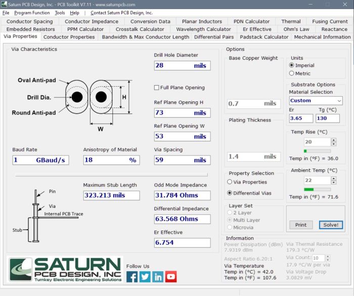
A simple 26 layer test vehicle was fabricated to compare the accuracy of the differential via circuit model to real vias. It consisted of two differential via pairs separated by 6 inches of 100 Ohm stripline differential pairs. Three sample via structures representing long, medium and short via stubs, as summarized in Figure 6, were measured using an Agilent N5230A VNA.
The differential vias had the following common parameters:
 Via drill diameter; D = 28 mils
Center to center pitch; s = 59 mils
Oval anti-pads= 53 mils x 73 mils
Dk of the laminate = 3.65
Anisotropy in Dkxy = 18%
Zvia = Zstub = 31.7 Ohms (per Equation 1)
Dkeff = 6.8 (per Equation 2)
Agilent ADS software was used to model and facilitate simulation correlation of the measured data as captured in Figure 7. This simple model accounts for the discontinuity of the long through section and the long stub section. The top half is the measured channel using an S-parameter file. The bottom half is a circuit model of the channel. Since the probes were not calibrated out, they are part of the device under test. The balun transformers are used to facilitate the display of the S-parameter and TDR results.
The comparison between the measured and simulated results of the insertion loss and TDR response for the three via stub cases using this simple approximation methodology is summarized in Figure 8. The insertion loss plots, in the frequency domain, are shown on the left, while the TDR plots are shown on the right.
The resonant nulls in the SDD21 plots are due to the stub lengths. As you can see, the longer the stub, the lower the resonant frequency null. If this null happens at the Nyquist frequency of the bit rate, the eye will be totally closed. This is why we back-drill them out after the board has been fabricated.
The simulation correlation is excellent up to about 12 GHz. The TDR plots show excellent impedance matching and delay for all three cases, while the simulated stub resonant frequencies match the measured frequencies very well. As you can see, these simple approximations for Dkeff and Zvia are perfectly adequate in providing a quick and accurate circuit model for differential through hole vias typically used in backplane applications.
Summary:
As illustrated, a simple twin-rod model (Figure 2) is used as the basis for a practical differential via circuit modeling methodology. By using Equation 1 and Equation 2, you can quickly determine the odd-mode impedance and effective dielectric constant needed for the circuit model.
Of course, you should use this methodology first as a rough starting point to quickly estimate the performance of your differential via design. If your worst case topology simulations show the performance is marginal, then it is worth while to invest the time and money to develop a 3D full wave model to perform a more accurate analysis.
On the other hand, if you find this approximation shows the vias have little impact on the channel performance, it may be of greater value for you to invest your time and money in resolving other critical issues with your design.
Try it the next time you are losing sleep over your design challenges.
For more Information:

If you liked this design note and want to learn more, or get more details on this innovative via modeling methodology, you can visit my web site, LAMSIM Enterprises.com , and download a copy of the white paper I wrote along with Eric Bogatin and Yazi Cao titled, “Method of Modeling Differential Vias” .
While you are there, feel free to investigate my other white papers and publications.
If you would like more information on our signal integrity and backplane services, or how we can help you achieve your next high-speed design challenge, email us at: info@lamsimenterprises.com.
UPDATE: In collaboration with Saturn PCB, I am pleased to announce my differential via equations above have been incorporated in a new impedance calculator available now in Saturn PCB Tool Kit software suite.
Twin-rod and Rod-over-plane Transmission Line Geometries
In my last Design Note on coaxial transmission geometry, I mentioned it was one of three unique cross-sectional geometries that have exact equations for inductance and capacitance. The other two are twin-rod and rod-over-plane. All three relationships assume the dielectric material is homogeneous and completely fills the space when there are electric fields.
A common application for twin-rod geometry is twin-lead ribbon cable; once used for RF transmission between antenna and TV sets. With the popularity of cable and satellite TV over the years, twin-lead has given way to coaxial cable due to its superior noise rejection and shielding effectiveness.
If we look at Figure1, we can see the electromagnetic field relationship of a twin-rod geometry when it is driven differentially. As current propagates along one rod, an equal and opposite current flows in the opposite direction along the other.
The right half of Figure 1 shows the magnetic-field loops and direction of rotation around each rod. Only one loop is shown for clarity, but the number of loops is a function of the amount of current and the length of the rods. The counter-rotating loops of current forms a virtual return at exactly one half of the space between the two rods. We call this a virtual return because if we were to put a conducting plane in the same position, the electromagnetic fields would look exactly the same.

Figure 1 Twin-rod geometry showing electromagnetic field relationship.
In his book, “Signal Integrity Simplified”, Eric Bogatin defines the loop inductance as, “the total number of field line loops around a conductor per amp of current”, and the loop self-inductance as, “the total number of field line loops around a conductor per amp of current in the same loop” . Applying these definitions to the figure, the loop inductance (L) is the inductance between the two rods, and the loop self-inductance (L/2) is the loop self inductance to the virtual return plane; equal to one half the loop inductance.
Likewise, the left half of Figure 1 shows the electric field with a capacitance (C) between the two rods, and twice the capacitance (2C) from each rod to the virtual return plane.
The relationships between capacitance, inductance and impedance of a twin-rod geometry are described by the following equations:

Where:
Ctwin = Capacitance between twin-rods – F
Ltwin = Loop Inductance between twin-rods – H
Zdiff = Differential impedance of twin-rods – Ω
Dk = Dielectric constant of material
Len = Length of the rods – inches
r = Radius of the rods – inches
s = Space between the rods – inches
Because the electro-magnetic fields create a virtual return plane at exactly one half of the spacing between the rods, each rod behaves like a single rod-over-plane geometry as illustrated in Figure 2.

Figure 2 Electromagnetic fields comparison of Twin-rod (left) vs. Rod-over-plane (right) geometries.
Whenever an AC current carrying conductor is in close proximity to a conducting plane, as is the case for rod-over-plane, some of the magnetic-field lines penetrate it. When the current changes direction, the associated magnetic-field lines also change direction; causing small voltages to be induced in the plane. These voltages create eddy currents, which in turn produce their own magnetic-fields.
Eddy current-induced magnetic-field line patterns look exactly like magnetic-field lines from an imaginary current below the plane; located the same distance as the real current above the plane. This imaginary current is called an image current, and has the same magnitude as the real current; except in the opposite direction [1]. The image current creates associated image magnetic-field lines in the opposite direction of the real field lines. As a result, the real magnetic-field lines are compressed between the rod and the plane. Since the rod-over-plane geometry has only one rod, the loop inductance is the same as the loop self-inductance.
For a twin-rod geometry, the odd mode capacitance is the capacitance of each rod to virtual return plane and is equal to twice the capacitance between rods.

Likewise, the odd mode inductance is the inductance of each rod to virtual return plane and equal to one half the inductance between rods.

The odd mode impedance of each rod is half of the differential impedance, and is equivalent to the rod-over-plane impedance.

[1] “Signal Integrity Simplified”, Eric Bogatin
