Archive for April 2024
PCB Laminate Anisotropy: The Impact on Advanced Via Modeling
Originally published in Signal Integrity Journal March 20, 2024.
As artificial intelligence (AI) and machine learning (ML) challenge engineers to process more data faster, electronic design automation (EDA) tools are progressively integrating AI and ML to advance the design process. Many refer to this process as “shifting-left” or “shift-left.”
Several EDA tools often boast about their capability to extract and simulate nets from a PCB design file with a simple click of a button. However, if the user is not cognizant of dielectric anisotropy, or if the software does not account for it, the simulation results may be inaccurate. This could pose a challenge for simulating the next generation 112/224 Gbps interconnect due to the shrinking of already tight margins.
In the process of modeling a PCB via, it is crucial to obtain accurate dielectric material properties from reliable sources. A key factor in this regard is relative permittivity, or dielectric constant (Dk).
Copper clad laminate (CCL) panels used for PCB fabrication are a mixture of fiberglass and resin, cladded on one or both sides with copper. CCL suppliers use various test methods to determine Dk and dissipation factor (Df), which are eventually published in their construction tables. PCB fabricators and signal integrity (SI) and power integrity (PI) engineers then rely on these values, which are used to design PCB stackups and perform SI/PI analysis.
There are over a dozen test methods specified in Institute of Printed Circuits (IPC) specifications. These test methods were designed as a means of testing for quality control in a production environment and do not guarantee the numbers are accurate for design applications. Usually, CCL suppliers include a footnote disclaimer with similar wording to that effect in their construction tables.
PCB Laminate Anisotropy
All glass weave reinforced laminates are anisotropic, meaning dielectric properties will be different along different axes. Unfortunately, the publication of Dk by CCL suppliers does not include anisotropic properties required for precise impedance prediction and SI modeling.
The values of Dk can be different based on the specific test method used. Some methods give results from in-plane measurements, where the electric fields are parallel to the test sample. Conversely, other methods derive Dk from out-of-plane measurements, where the electric fields are perpendicular to the test sample.
Figure 1a shows a block of fiberglass reinforced laminate, with the glass weave and copper plates running parallel to the x-y axis. When a DC potential is applied, a uniform electric field is out-of-plane in the z-direction, thereby creating a capacitor. Since the effective Dk is the ratio of actual structure’s capacitance, to the capacitance when the dielectric is replaced by air, we denote this ratio as Dkz.
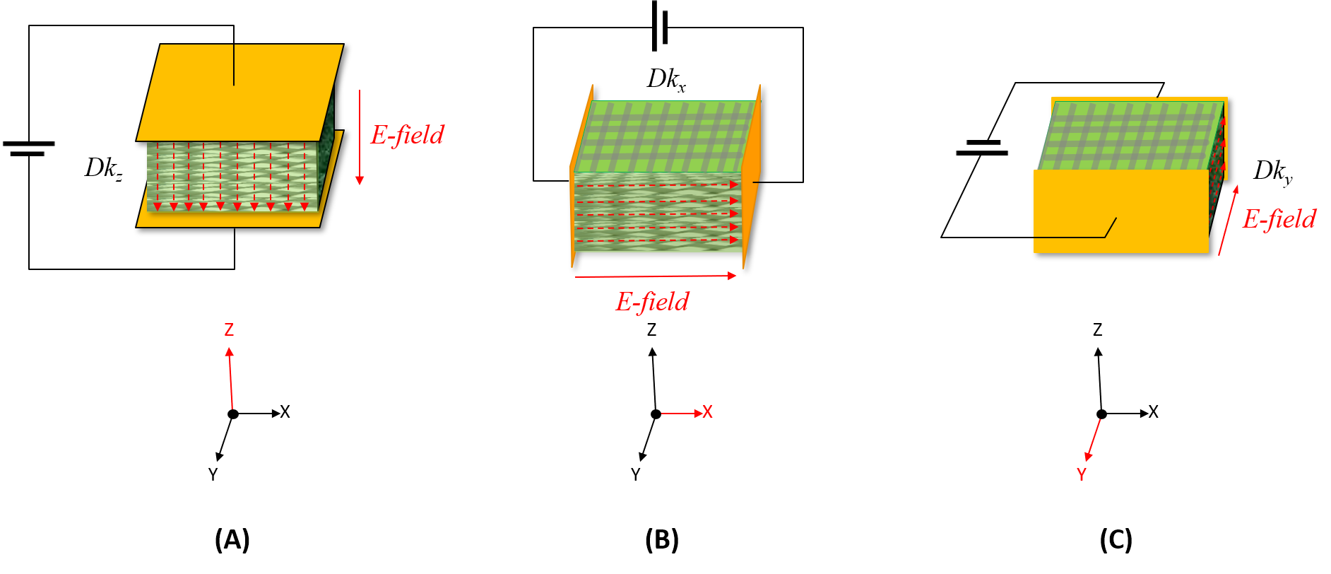
Figure 1. E-field orientation relative to the glass weave reinforcement in PCB laminates when a DC electrical potential is applied: E-fields are out-of-plane with respect to the glass weave (A) and in-plane with the glass weave (B, C).
Figure 1b and 1c show that when the conducting plates are placed perpendicular to the direction of the glass weave, the E-fields align with the x or y axis and are in-plane. Even though there might be slight variations in the effective Dk in these directions, heuristically we assume they are equal and refer to them as Dkxy.
Depending on the test method used, Dk measured may be different due to the test fixture’s generated E-field orientation relative to the glass weave. Figure 2 summarizes E-field orientation when compared against popular test methods used by CCL suppliers. Dk obtained by these test methods are denoted as in-plane (Dkxy) or out-of-plane (Dkz).
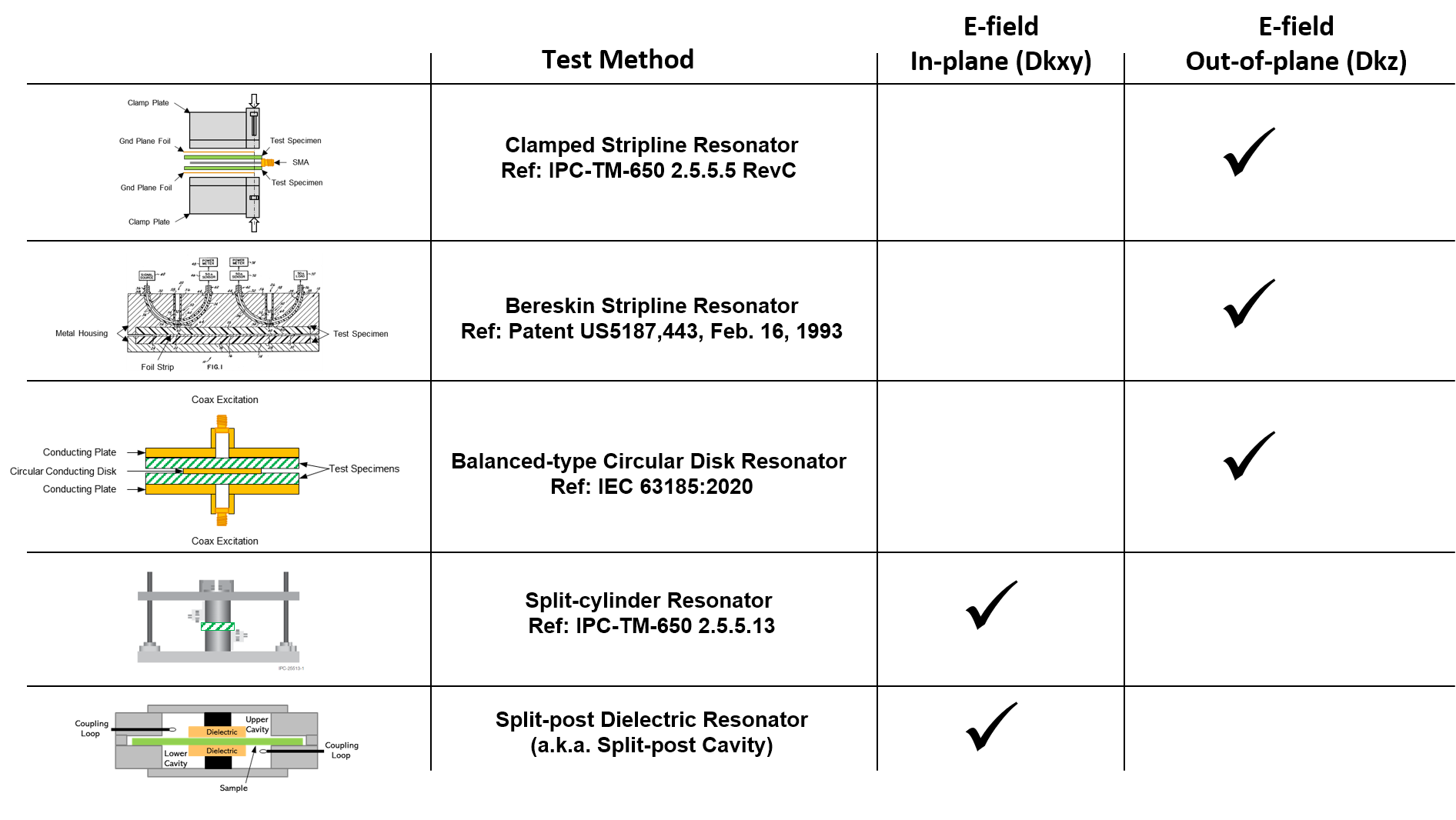
Figure 2. Comparative table of E-field orientation and resulting Dkxy or Dkz across popular test methods employed by CCL suppliers.
Dkxy is typically higher compared to Dkz, depending on the glass resin mixtures of the sample tested as shown in Figure 3a.

Figure 3. Rule of solid mixtures: Parallel mixing rule is used when E-fields are polarized in Z-direction (A) and series mixing rule is used when E-fields are polarized in x-y direction (B).
The rules of solid mixtures1 can be used to estimate anisotropy of the glass and resin mixture. If the E-field is polarized in the z-direction, using a Dk of 6.8 for E-glass (Dkg), a Dk of 2.5 for resin (Dkr), volume fraction of resin (vresin = 0.7), and volume fraction of E-glass (vglass = 0.3), then the effective capacitance of each block is in series and Dkz is determined to be 3.09, using the parallel mixing rule defined by:

When the conductor plates are moved, as shown in Figure 3b, and the mixture is polarized such that the E-field is parallel to the x-y axis, then the effective capacitance is in parallel and Dkxy is determined to be 3.79, using the series mixing rule defined by:

Using Equation 3, Anisotropy (Λ) of the mixture reveals that Dkxy is 23% higher than Dkz.

Anisotropy Implications for Via Modeling
PCB transmission lines run parallel to the glass weave and E-fields are predominantly out-of-plane. Thus, Dkz is needed for accurate impedance modeling. Using Dkxy instead means the impedance predicted from the field solver will be lower than what would be measured if the board was made exactly as specified in the stackup.
In the case of modeling vias, it gets more complicated. In Figure 4, given a cross-section view of a typical via and stub, we observe the E-fields as the signal propagates, from left to right, along the microstrip transmission line on the top layer, through the via to an inner stripline layer 3 and continuing through the stub.

Figure 4. Cross-section view of E-fields as a 20 GHz signal propagates from the microstrip top layer through a via with stub to a stripline layer 3 (HFSS simulation courtesy of Juliano Mologni, Ansys4).
Using the same value for Dk when modeling transmission lines and vias leads to inaccurate results for one or the other. If the CCL supplier’s published numbers are out-of-plane, Dkz, then the impedance for transmission lines will be correct, while the via impedance will end up being lower than modeled. On the other hand, if the published numbers are in-plane, Dkxy, then the via impedance will be correct and the transmission line impedance will end up being higher.
Furthermore, using the wrong Dk for modeling via stubs will result in poor simulation correlation to measurements2 and potentially the loss of channel margin due to maximum stub length guidelines based on simulation analysis.3 This can be problematic for 112/224 Gbps interconnects by reducing already tight margins.
Figure 5 shows an example of this issue. A 26 mil (0.66 mm) pitch differential via with a 10 mil (0.254 mm) stub model was created in Keysight ADS5 via designer (see Figure 5a). A Dkz of 3.09 and Dkxy of 3.79 from Equation 1 and Equation 2 were used in the model for comparisons. After finite element method (FEM) simulation, S-parameters were saved in touchstone format and simulated in the circuit schematic shown in Figure 5b.

Figure 5. Simulated results for differential IL/RL (C) and TDR impedance (D) of a differential via model with 10 mil (0.254 mm) stub using Dkz of 3.09 (red plots) and Dkxy of 3.79 (blue plots) for laminate. Modeled and simulated with Keysight ADS5 via designer.
Figure 5c compares differential insertion loss (IL) and return loss (RL) and Figure 5d compares differential time domain reflectometer (TDR) impedance. The red plots are using out-of-plane Dkz and the blue plots are using in-plane Dkxy. As can be seen, when out-of-plane Dkz value is used in the model, it underestimates IL and impedance by approximately 8 Ohm. For 112 Gbps, the difference in loss at 28 GHz Nyquist frequency is ~ 0.3 dB. At 56 GHz Nyquist for 224 Gbps, the delta is ~ 0.9 dB, caused by the difference in stub resonant nulls at 106 and 95 GHz.
But this doesn’t tell the whole story. While it is widely known that short, highly reflective channels can negatively impact channel performance, the issue has been exacerbated by the introduction of 4-level pulse amplitude modulated (PAM4) signaling, which reduces the signal-noise ratio by 9.5 dB. As bit rates continue to increase exponentially, traditional IL/RL masks and eye diagrams are no longer sufficient for assessing channel quality.
Channel operating margin (COM)7 is a system-level metric approach adopted by the IEEE 802.3ck standard to validate the performance of a serial link. As part of COM, there is an effective return loss (ERL) metric that factors in reflections caused by impedance mismatches at the pins of the transmitter, receiver, and any other discontinuities between them. Thus, COM can be used to assess the impact of Dk anisotropy on key metrics.
A short channel representing a typical chip-to-chip (C2C) topology was modeled by concatenating touchstone files for vias and transmission lines using Keysight ADS5, as depicted in Figure 6b. The 2 in. (5.08 cm), 100 Ohm differential transmission line was modeled with Polar SI90006 using an out-of-plane Dkz value of 3.09.

Figure 6. Simulated TDR and COM results when Dkz was used for vias and transmission lines compared to when Dkxy was used for via models and Dkz used for transmission lines. When Dkz was used for all models COM and ERL passed (d), but when Dkxy was used for the via models, COM passes with reduced margins and ERL failed (E).
Figure 6a shows the differential TDR response obtained using a Dkz value of 3.09 for the via and transmission line models. As shown in Figure 6d, both COM and ERL passed when a short package model was used. When the via files were replaced with files modeled with Dkxy of 3.79, the differential TDR response is degraded, as shown in Figure 6c. Figure 6e shows that although COM passed, it had reduced margins and ERL failed.
Of course, this was an extreme example with high Dk anisotropy. Choosing a dielectric with low Dk glass and higher resin content would improve the results. But if you have a tight loss budget to begin with, using the wrong numbers could cause failure to meet compliance once your board is built and tested.
Summary
Since woven glass PCB substrates are anisotropic, EDA design and modeling software hoping to advance AI and ML algorithms should have provisions to model anisotropic material, especially via transitions.
It is important to have awareness of the test method used by CCL suppliers for accurate modeling and simulation. Using out-of-plane Dkz values instead of in-plane Dkxy values for via modeling can cause misleading simulation results, which may result in reduced margins and potential compliance test failures when the design is built and tested.
It is recommended that CCL suppliers provide anisotropic properties in their Dk/Df construction tables. In lieu of that, my DesignCon 2024 paper and presentation titled “A Heuristic Approach to Assess Anisotropic Properties of Glass-reinforced PCB Substrates” will be delving deeper into anisotropy to reveal how to calculate anisotropy from CCL suppliers’ Dk/Df construction tables. The full paper will be made available following the event.
April 3, 2024 update: The DesignCon paper is now available on my web site:

REFERENCES
-
P. S. Neelakanta, “Handbook of Electromagnetic Materials: Monolithic and Composite Versions and Their Applications,” CRC Press LLC, 1995.
-
L. Simonovich, E. Bogatin, and Y. Cao, “Differential Via Modeling Methodology,” IEEE Transactions on Components, Packaging and Manufacturing Technology, Vol. 1, No. 5, pp. 722–730, May 2011, doi: 10.1109/TCPMT.2010.2103313.
-
B. Simonovich, “Via Stubs – Are They all Bad?”, Signal Integrity Journal, March 10, 2017
-
ANSYS, Inc. Headquarters, Southpointe, 2600 Ansys Drive, Canonsburg, Pa., 15317, U.S.
-
Keysight PathWave Advanced Design System (ADS) [computer software], (Version 2023, Update 2).
-
Polar Instruments Si9000 [computer software], (Version 22.09.01).
-
IEEE802.3ck COM v3.70, computer software.
