Archive for the ‘Modeling’ Category
Via Stubs Demystified
 We worry about via stubs in high-speed designs because they cause unwanted resonant frequency nulls which appear in the insertion loss plot (IL) of the channel. But are all via stubs bad? Well, as with most answers relating to signal integrity, “It depends.”
If one of these frequency nulls happen to line up at or near the Nyquist frequency of the bit- rate (i.e. 1/2 of the bit-rate), the received eye will be devastated, resulting in a high bit-error-ratio (BER), or even link failure.
Figure 1 shows simulation results of two backplane channels. On the left are measured SDD21 insertion loss and eye diagram of a 10 GB/s, non-return-to-zero (NRZ) signal, with short through vias and long stubs ~ 270 mils. On the right, shows measured SDD21 IL and eye diagram of a channel with long through vias and shorter stubs ~ 65 mils
Because the ¼ -wave resonant null occurs at a frequency ~ 4. 4 GHz, this is near the Nyquist frequency for 10 GB/s. As can be seen, the eye is totally closed for the long stub case. But when the shorter stub case is simulated, the eye is open with plenty of margin.
So how does a via stub cause ¼ -wave resonance? This question can be explained with the aid of Figure 2. Starting on the left, we see a via with two sections. The through (thru) part is the top portion connecting a device pin to an inner layer trace of a printed circuit board (PCB). The stub portion is the lower portion and is an open circuit.
On the right a sinusoidal signal is injected into the pin at the top of the via and travels along the thru portion until it reaches the junction of the internal trace and stub. At that point, the signal splits. Some of it travels along the trace, and the rest continues down the stub. Once it reaches the bottom, it reflects back up. When it reaches the trace junction, it splits again with a portion traveling along the trace and the rest back to the source.
If f is the frequency of a sine wave, and the time delay (TD) through the stub portion equals a ¼ -wavelength, then when it reflects at the bottom and reaches the junction again, it will be delayed by ½ a cycle and cancels most of the original signal.

Figure 2 Illustration of a ¼ -wave resonance of a stub. If f = frequency where TD = ¼ wavelength, then when 2TD = ½ cycle minimum signal received.
Resonance nulls occurs at the fundamental frequency ( fo) and at every odd harmonic. If you know the length of the stub (in inches) and the effective dielectric constant (Dkeff), surrounding the via hole structure, the resonant frequency can be predicted by:
Equation 1

Where: fo is the ¼ -wave resonant frequency (GHz); c is the speed of light (~11.8 in/ns); Stub_length is inches.
You will find that Dkeff is not the same as the bulk Dk published in laminate manufacturers’ data sheets. It is typically higher. A higher Dkeff increases phase delay through the via resulting in a lower resonant frequency.
One reason is excess capacitance from the via pads as well as the via barrel’s proximity to the clearance hole openings (also known as anti-pads) in plane layers. The other is because of the anisotropic nature of the laminate material.
For the example in Figure 1, the ¼ -wave resonant frequency of the long via stub is ~ 4.4 GHz. With a stub length of ~ 270 mils, this gives a Dkeff of 6.16, which is considerably higher than the published bulk Dk of 3.65. When you model a via in an electro-magnetic (EM) 3D field solver, it automatically accounts for the excess capacitance, but you will still need to compensate for the anisotropic nature of the dielectric.
A material is anisotropic when there are different values for parallel (x-y) vs perpendicular (z) measured values for dielectric constant. Dielectric constant and loss tangent, as published in manufacturers’ data sheets, report perpendicular measured values. For FR-4 fiberglass reinforced laminates, anisotropy can range from 15% -25% higher. The bad news is these numbers are not readily available from data sheets.
For differentially driven vias with plane layers evenly distributed throughout the entire stackup, Dkeff can be roughly estimated by:
Equation 2

Where: Dkxy is the dielectric constant adjusted for anisotropy (15%-25% higher); Dkz is the bulk dielectric constant from data sheets; s is via-via spacing; drillØ is drill diameter; H and W are anti-pad shape dimensions as shown in Figure 3 .

Figure 3 Anti-pad parameters for Equation 2.
The effects of via stubs can be mitigated by: using blind or buried vias; back-drilling; or by using thru vias only (i.e. from top layer to bottom layer). Practically, the shortest stub that can be achieved by back-drilling is on the order of 5 to 10 mils.
As a rule of thumb, we usually strive to have an interconnect bandwidth (BW) to be five times the Nyquist frequency of the bit-rate. Since a ¼-wave resonant null behaves somewhat like a notch filter, depending on the high-frequency roll-off due to Q-factor, frequencies near resonance will be attenuated. For that reason a good rule of thumb to follow is making sure the first null should occur at the 7th harmonic, or higher, of the Nyquist frequency to maintain the integrity of the 5th harmonic frequency component that makes up the risetime of a signal.
With this in mind, for a given baud-rate (Baud) in GBd, the maximum stub length (lmax), in inches can be estimated by:
Equation 3

For NRZ signaling, the baud-rate is equal to the bit rate. But for pulse-amplitude modulation (PAM-4) signaling, which has 2 symbols per bit time, the baud-rate is ½ of that. Thus a 56 GB/s PAM-4 signal has a baud-rate of 28 GBd, and the Nyquist frequency is 14 GHz, which happens to be the same as 28 GB/s NRZ signalling.
Figure 4 presents a chart of maximum stub length vs baud-rate based on Equation 3, using a Dkeff = 6.16 (blue) vs 3.65 (red). It shows us the higher the baud-rate, the more the stub length becomes an issue, especially past 10 GBd. We also get a feel for the sensitivity of stub length to Dkeff . Even though there is ~ 70% difference in Dkeff, there is only ~ 30% delta in stub lengths for the same baud-rate. This means that even if we use the bulk Dk published in data sheets, we are probably not dead in the water.
If the respective stub length is greater than this, it does not mean there is a show stopper. Depending on how much longer means the eye opening at the receiver will be degraded and we lose margin. We see this by the example in Figure 1. Even though the stub lengths in the channel were almost double the value at 10 GBd from the chart, there is still plenty of eye opening.

Figure 4 Chart showing estimated maximum stub length vs baud-rate with Dkeff of 6.16 (red) vs 3.65 (blue) based on Equation 3
To further explore design space and test out the rule of thumb, a generic circuit model was built using Keysight ADS with the ability to vary the via stub lengths
Referring to the chart, at 28 GBd, the maximum stub length should be 12 mils, assuming a Dkeff of 6.16. Figure 5 shows simulation results for NRZ signalling. As can be seen, there was a difference of only 17 mV in eye height (1.5%), and no extra jitter for 12 mil stubs compared to 5 mil stubs.

Figure 5 Eye diagrams comparison with BER at 10E-12 for stub lengths of 5 mils vs 12 mils. Modeled and simulated with Keysight ADS.
But if we use the exact same channel model, and use the generic PAM-4 IBIS AMI model from Keysight Technologies, we can see the results plotted in Figure 6. On the left are the eye openings with 5 mil stubs and the right with 12 mil stubs. In this case, there was an average reduction of ~7 mV (6%) in eye heights, and 0.24 ps (2%) in eye widths at BER 10E-12 across all three eyes.

Figure 6 PAM-4, 28 GBd (56 GB/s) eye height and width comparison at BER of 10E-12 for 5 mil vs 12 mil stub lengths. Modeled and simulated with Keysight ADS.
Because PAM-4 signalling has three smaller eyes, that are one-third the size of an NRZ eye for the same amplitude, it is more sensitive to channel impairments. From the above examples, we can see NRZ had only 1.5% reduction in eye height compared to 6% for PAM-4. Similarly there was no increase in jitter for NRZ compared to 2% increase for PAM-4 when stub lengths changed from 5 mils to 12 mils.
What this says is maintaining a BW to 5 times Nyquist rule of thumb, when estimating via stub lengths, is quite conservative for NRZ signalling. There is almost the same BW as the channel with 5 mil stub, which was the original objective. But because PAM-4 is more sensitive to impairments, it shows there is less margin.
In summary then, rules of thumb and related equations are a good way to reinforce your intuitions or to give you an answer sooner rather than later. They help you know what to expect before you take any measurements or perform any simulations. But they should never be used to sign off on any high-speed design.
Because every system will have different impairments affecting BER, the only way to know how much margin you have is by modeling the via with a 3-D EM field solver, based on the actual stackup and simulating the entire channel complete with crosstalk, if margins are tight. This is even more critical for data rates above 10 GBd.
So to answer the original question, “are all via stubs bad”? Well, the answer is it still depends. For NRZ signalling, there is more leeway than for PAM-4. But you now have a practical way to quickly quantify the answer if you know the stub length, baud-rate and delay through the via.
Obsessions with Conductor Surface Roughness – What’s the Dk Because of it?
 You know you have an obsession when you are flying 6 miles over Colorado; look out your window at the beautiful scenery; and all you can think about is how the rocky mountain topology reminds you of conductor surface roughness! Well call me obsessed because that’s exactly what I thought on my way to DesignCon 2017 in Santa Clara, CA.
For those of you who know me, you know that I have been researching practical methods to model conductor surface roughness, and its effect on insertion loss (IL). I have presented several papers on the subject over the last couple of years. It’s one of my pet projects. This year, at DesignCon, I presented a paper titled, “A Practical Method to Model Effective Permittivity and Phase Delay Due to Conductor Surface Roughness” .
Everyone involved in the design and manufacture of printed circuit boards (PCBs) knows one of the most important properties of the dielectric material is the relative permittivity (εr), commonly referred to as dielectric constant (Dk). But in reality, Dk is not constant at all. It varies over frequency as you will see later.
We often assume the value reported in manufacturers’ data sheets is the intrinsic property of the material. But in actual fact, it is the effective dielectric constant (Dkeff) generated by a specific test method. When you compare simulation against measurements, you will often see a discrepancy in Dkeff and IL, due to increased phase delay caused by surface roughness. This has always bothered me. For a long time I was always looking for ways to come up with Dkeff from data sheet numbers alone. Thus the obsession and motivation for my recent research work.
Since phase delay, also known as time delay (TD), is proportional to Dkeff of the material, my theory was that the surface roughness profile decreases the effective separation between parallel plates, thereby increasing the electric field (e-field) strength, resulting in additional capacitance, which accounts for an increase in effective Dk and TD.
The main focus of my paper was to prove the theory and to show a practical method to model Dkeff and TD due to surface roughness. By referencing Gauss’s Law for charged parallel plates, I confirmed mathematically, and through simulation, how the dielectric thickness and permittivity are interrelated to e-field and capacitance. I also revealed how the 10-point mean (Rz) roughness parameter can be applied to finally estimate effective Dkeff due to roughness. Finally I tested the method via case studies.
In his book, “Transmission Line Design Handbook”, Wadell defines Dkeff as the ratio of the actual structure’s capacitance to the capacitance when the dielectric is replaced by air.
Dkeff is highly dependent on the test apparatus and conditions of how it is measured. There are several methods used in the industry. One method that is commonly used by many laminate suppliers is called the clamped stripline resonator test method. It is described by IPC-TM-650, section 2.5.5.5, Rev C.
In short, this method rapidly tests dielectric material for permittivity and loss tangent, over an X-band frequency range of 8-12.4 GHz, in a production environment. It does not guarantee the values are accurate for design applications.
Here’s why:
The measurements are made under stripline conditions, using a carefully designed resonant element pattern card, made out of the same dielectric material to be tested. The card is sandwiched between two sheets of unclad dielectric material under test. The whole structure is then clamped between two large plates, lined with copper foils that are grounded.
Since the resonant element pattern card and material under test are not physically bonded together, there are small air gaps between the various layers affecting measured results. These air gaps are caused in part by:
- Removing the copper from the material under test, leaving the bare substrate, complete with the micro void imprint of the copper roughness.
- The air gap between resonant element pattern card and material under test, due to the copper thickness of the etch pattern.
- The roughness profile of the copper, on the resonant element pattern card and fixture’s grounded foil reference planes, are different than would be in practice, unless the same foil type is used.
If Dkeff and Rz roughness parameters from the manufacturers’ data sheets are known, then the effective Dk due to roughness (Dkeff_rough) of the fabricated core laminate can now be easily estimated by:

Where: Hsmooth is the thickness of dielectric from data sheet; Rz is 10-point mean roughness from data sheet; and Dkeff is the Dk from data sheet.
With reference to Figure 1, using Dkeff with rough copper model, as shown on the left, is equivalent to using Dkeff_rough, with smooth copper model, as shown on the right. Therefore all you need to do is use Dkeff_rough for impedance calculations, and any other numerical simulations based on surface roughness, instead of Dk published in data sheets.
It is as simple as that.

Figure 1 Effective Dk due to roughness model. Using Dkeff with rough copper model (left) is equivalent to using Dkeff_rough with smooth copper model (right).
For example, one case study I presented used measurements from a CMP28 modeling platform from Wild River Technology. The PCB was fabricated with FR408HR material and reverse treated foil (RTF). Keysight EEsof EDA ADS software was used for modeling and simulation. The results are shown in Figure 2.
The left graph shows results when data sheet values for core and prepreg were used. Dkeff measured (red) was 3.761, compared to simulated Dkeff (blue) of 3.626, at 10 GHz. This gave a delta of ~ 4%. But when the Dkeff_rough was used for core and prepreg the delta was within 1%.

Figure 2 Measured vs simulated Dkeff using FR408HR data sheet values for core and prepreg (left) and using Dkeff_rough (right). Modeled and simulated with Keysight EEsof EDA ADS software.
The paper shows in more detail how Equation 1 was derived, based on Gauss’ Law. In addition, I show how IL and phase delay is also improved when Dkeff_rough is used instead of data sheet values. You can download the paper titled, “A Practical Method to Model Effective Permittivity and Phase Delay Due to Conductor Surface Roughness”, and other papers on modeling conductor loss due to roughness from my web site.
Practical Conductor Roughness Modeling with Cannonballs

In the GB/s regime, accurate modeling of conductor losses is a precursor to successful high-speed serial link designs. Failure to model roughness effects can ruin you day. For example, Figure 1 shows the simulated total loss of a 40 inch printed circuit board (PCB) trace without roughness compared to measured data. Total loss is the sum of dielectric and conductor losses. With just -3dB delta in insertion loss between simulated and measured data at 12.5 GHz, there is half the eye height opening with rough copper at 25GB/s.
So what do cannon balls have to do with modeling copper roughness anyway? Well, other than sharing the principle of close packing of equal spheres, and having a cool name, not very much.
According to Wikipedia, close-packing of equal spheres is defined as “a dense arrangement of congruent spheres in an infinite, regular arrangement (or lattice)” [8]. The cubic close-packed and hexagonal close-packed are examples of two regular lattices. The cannonball stack is an example of a cubic close-packing of equal spheres, and is the basis of modeling the surface roughness of a conductor in this design note.

Figure 1 Comparisons of measured insertion loss of a 40 inch trace vs simulation. Eye diagrams show that with -3dB delta in insertion loss at 12.5GHz there is half the eye opening at 25GB/s. Modeled and simulated with Keysight EEsof EDA ADS software [14].
Background
In printed circuit (PCB) construction there is no such thing as a perfectly smooth conductor surface. There is always some degree of roughness that promotes adhesion to the dielectric material. Unfortunately this roughness also contributes to additional conductor loss.
Electro-deposited (ED) copper is widely used in the PCB industry. A finished sheet of ED copper foil has a matte side and drum side. The drum side is always smoother than the matte side.
The matte side is usually attached to the core laminate. For high frequency boards, sometimes the drum side of the foil is laminated to the core. In this case it is referred to as reversed treated (RT) foil.
Various foil manufacturers offer ED copper foils with varying degrees of roughness. Each supplier tends to market their product with their own brand name. Presently, there seems to be three distinct classes of copper foil roughness:
· Standard
· Very-low profile (VLP)
· Ultra-low profile (ULP) or profile free (PF)
Some other common names referring to ULP class are HVLP or eVLP.
Profilometers are often used to quantify the roughness tooth profile of electro-deposited copper. Tooth profiles are typically reported in terms of 10-point mean roughness (Rz ) for both sides, but sometimes the drum side reports average roughness (Ra ) in manufacturers’ data sheets. Some manufacturers also report RMS roughness (Rq ).
Modeling Roughness
Several modeling methods were developed over the years to determine a roughness correction factor (KSR ). When multiplicatively applied to the smooth conductor attenuation (αsmooth ), the attenuation due to roughness (αrough ) can be determined by:
Equation 1
![]()
The most popular method, for years, has been the Hammerstad and Jensen (H&J) model, based on work done in 1949 by S. P. Morgan. The H&J roughness correction factor (KHJ ), at a particular frequency, is solely based on a mathematical fit to S. P. Morgan’s power loss data and is determined by [2]:
Equation 2

Where:
KHJ = H&J roughness correction factor;
∆ = RMS tooth height in meters;
δ = skin depth in meters.
Alternating current (AC) causes conductor loss to increase in proportion to the square root of frequency. This is due to the redistribution of current towards the outer edges caused by skin-effect. The resulting skin-depth (δ ) is the effective thickness where the current flows around the perimeter and is a function of frequency.
Skin-depth at a particular frequency is determined by:
Equation 3

Where:
δ = skin-depth in meters;
f = sine-wave frequency in Hz;
μ0= permeability of free space =1.256E-6 Wb/A-m;
σ = conductivity in S/m. For annealed copper σ = 5.80E7 S/m.
The model has correlated well for microstrip geometries up to about 15 GHz, for surface roughness of less than 2 RMS. However, it proved less accurate for frequencies above about 5GHz for very rough copper [3] .
In recent years, the Huray model [4] has gained popularity due to the continually increasing data rate’s need for better modeling accuracy. It takes a real world physics approach to explain losses due to surface roughness. The model is based on a non-uniform distribution of spherical shapes resembling “snowballs” and stacked together forming a pyramidal geometry, as shown by the scanning electron microscope (SEM) photo in Figure 2.

Figure 2 SEM photograph of electrodeposited copper nodules on a matte surface resembling “snowballs” on top of heat treated base foil. Photo credit Oak-Mitsui.
By applying electromagnetic wave analysis, the superposition of the sphere losses can be used to calculate the total loss of the structure. Since the losses are proportional to the surface area of the roughness profile, an accurate estimation of a roughness correction factor (KSRH) can be analytically solved by [1]:
Equation 4

Where:
KSRH (f ) = roughness correction factor, as a function of frequency, due to surface roughness based on the Huray model;
Aflat= relative area of the matte base compared to a flat surface;
ai = radius of the copper sphere (snowball) of the ith size, in meters;
Ni = number of copper spheres of the ith size per unit flat area in sq. meters;
δ (f ) = skin-depth, as a function of frequency, in meters.
Simonovich-Cannonball Model
Using the concept of cubic close-packing of equal spheres, the radius of the spheres (ai ) and tile area (Aflat ) parameters for the Huray model can now be determined solely by the roughness parameters published in manufacturers’ data sheets.
Why is this important? Well, as my friend Eric Bogatin often says, “Sometimes an OK answer NOW! is more important than a good answer late”. For example, often during the architectural phase of a backplane design, you are going through some what-if scenarios to decide on a final physical configuration. Having a method to accurately predict loss from data sheets alone rather than go through a design feedback method, described in [7] can save an enormous amount of time and money.
Another reason is that it gives you a sense of intuition on what to expect with measurements to help determine root cause of differences; or sanitize simulation results from commercial modeling tools. If you are like me, I always like to have alternate ways to verify that I have used the tool properly.
Recalling that losses are proportional to the surface area of the roughness profile, the Cannonball model can be used to optimally represent the surface roughness. As illustrated in Figure 3, there are three rows of spheres stacked on a square tile base. Nine spheres are on the first row, four spheres in the middle row, and one sphere on top.

Figure 3 Cannonball model showing a stack of 14 uniform size spheres (left). Top and front views (right) shows the area (Aflat) of base, height (HRMS) and radius of sphere (r).
Because the Cannonball model assumes the ratio of Amatte/Aflat = 1, and there are 14 spheres, Equation 4 can be simplified to:
Equation 5

Where:
KSR (f ) = roughness correction factor, as a function of frequency, due to surface roughness based on the Cannonball model;
r = sphere radius in meters; δ (f ) = skin-depth, as a function of frequency in meters;
Aflat = area of square tile base surrounding the 9 base spheres in sq. meters.
In my white paper [16] the radius of a single sphere is:

And the area of the square flat base is:
![]()
You can approximate the RMS heights of the drum and matte sides by Equation 6 and Equation 7 below:
Equation 6

Where: Rz_drum is the 10-point mean roughness in meters.
Equation 7

Where: Rz_matte is the 10-point mean roughness in meters.
Practical Example
To test the accuracy of the model, board parameters from a PCBDesign007 February 2014 article, by Yuriy Shlepnev [5] was used. Measured data was obtained from Simbeor software design examples courtesy of Simberian Inc. [9]. The extracted de-embedded generalized modal S-parameter (GMS) data was computed from 2 inch and 8 inch single-ended stripline traces. They were originally measured from the CMP-28 40 GHz High-Speed Channel Modeling Platform from Wild River Technology [14].
 The CMP-28 Channel Modeling Platform, (Figure 4 left -credit Wild River Technology) is a powerful tool for development of high-speed systems up to 40 GHz, and is an excellent platform for model development and analysis. It contains a total of 27 microstrip and stripline interconnect structures. All are equipped with 2.92mm connectors to facilitate accurate measurements with a vector network analyzer (VNA).
The PCB was fabricated with Isola FR408HR material and reverse treated (RT) 1oz. foil. The dielectric constant (Dk) and dissipation factor (Df), at 10GHz for FR408HR 3313 material, was obtained from Isola’s isoStack® web-based online design tool [10]. This tool is a free, but you need to register to use it. An example is shown in Figure 5.
Typical traces usually have a trapezoidal cross-section after etching due to etch factor. Since the tool does not handle trapezoidal cross-sections in the impedance calculation, an equivalent rectangular trace width was determined based on a 2:1 etch-factor (60 deg taper). The as designed nominal trace width of 11 mils, and a 1oz trace thickness of 1.25 mils per isoStack® was used in the analysis.

Figure 5 Example of Isola’s isoStack® online software used to determine dielectric thicknesses, Dk, Df and characteristic impedance for the CMP-28 board.
The default foil used on FR408HR core laminates is MLS, Grade 3, controlled elongation RT foil. The roughness parameters were easily obtained from Oak-mitsui [11]. Reviewing the data sheet, 1 oz. copper roughness parameters Rz for drum and matte sides are 120μin (3.175 μm) and 225μin (5.715μm) respectively. Because this is RT foil, the drum side is the treated side and bonded to the core laminate.
An oxide or micro-etch treatment is usually applied to the copper surfaces prior to final lamination. This provides enhanced adhesion to the prepreg material. CO-BRA BOND® [12] or MultiBond MP [13] are two examples of oxide alternative micro-etch treatments commonly used in the industry. Typically 50 μin (1.27μm) of copper is removed when the treatment is completed. But depending on the board shop’s process control, this can be 70-100 μin (1.78-2.54μm) or higher.
The etch treatment creates a surface full of micro-voids which follows the underlying rough profile and allows the resin to squish in and fill the voids providing a good anchor. Because some of the copper is removed during the micro-etch treatment, we need to reduce the published roughness parameter of the matte side by nominal 50 μin (1.27 μm) for a new thickness of 175μin (4.443μm).
Figure 6 shows SEM photos of typical surfaces for MLS RT foil courtesy of Oak-mitsui. The left and center photos are the treated drum side and untreated matte side respectively. The right photo is a 5000x SEM photo of the matte side showing micro-voids after etch treatment.

Figure 6 Example SEM photos of MLS RT foil courtesy of Oak-mitsui. Left is the treated drum side and center is untreated matte side. SEM photo on the right is the matte side after etch treatment.
The data sheet and design parameters are summarized in Table 1. Respective Dk, Df, core, prepreg and trace thickness were obtained from the isoStack® software, shown in Figure 5. Roughness parameters were obtained from Oak-mitsui data sheet. Rz of the matte side after micro-etch treatment (Rz = 4.443μm) was used to determine KSR_matte .
Table 1 CMP-28 test board parameters obtained from manufacturers’ data sheets and design objective.
|
Parameter |
FR408HR |
|
Dk Core/Prepreg |
3.65/3.59 @10GHz |
|
Df Core/Prepreg |
0.0094/0.0095 @ 10GHz |
|
Rz Drum side |
3.048 μm |
|
Rz Matte side before Micro-etch |
5.715 μm |
|
Rz Matte side after Micro-etch |
4.443 μm |
|
Trace Thickness, t |
31.730 μm |
|
Trace Etch Factor |
2:1 (60 deg taper) |
|
Trace Width, w |
11 mils (279.20 μm) |
|
Core thickness, H1 |
12 mils (304.60 μm) |
|
Prepreg thickness, H2 |
10.6 mils (269.00 μm) |
|
GMS trace length |
6 in (15.23 cm) |
Keysight EEsof EDA ADS software [14] was used for modeling and simulation analysis. A new controlled impedance line (CIL) designer enhancement, in version 2015.01, makes modeling the transmission line substrate easy. Unlike earlier substrate models, the CIL model allows you to model trapezoidal traces.
Figure 7 is the general schematic used for analysis. There are three transmission line substrates; one for dielectric loss; one for conductor loss and the other for total loss without roughness.

Figure 7 Keysight EEsof EDA ADS generic schematic of controlled impedance line designer used in the modeling and simulation analysis.
Dielectric loss was modeled using the Svensson/Djordjevic wideband Debye model to ensure causality. By setting the conductivity parameter to a value much-much greater than the normal conductivity of copper ensures the conductor is lossless for the simulation. Similarly the conductor loss model sets the Df to zero to ensure lossless dielectric.
Total insertion loss (IL) of the PCB trace, as a function of frequency, is the sum of dielectric and rough conductor insertion losses.
Equation 8
![]()
To accurately model the effect of roughness, the respective roughness correction factor (KSR ) must be multiplicatively applied to the AC resistance of the drum and matte sides of the traces separately. Unfortunately ADS, and many other commercial simulators, do not allow access to these surfaces to apply the correction properly. The best you can do is to apply the average of (KSR_drum ) and (KSR_matte ) side to the smooth conductor loss (ILsmooth ), as described above.
The following are the steps to determine KSR_avg (f ) and total IL with roughness:
1. Determine HRMS_drum and HRMS_matte from Equation 6 and Equation 7.

2. Determine the radius of spheres for drum and matte sides:

3. Determine the area of the square flat base for drum and matte sides:

4. Determine KSR_drum (f ) and KSR_matte (f ) :

5. Determine the average KSR_drum (f ) and KSR_matte (f ):

6. Apply Equation 8 to determine total insertion loss of the PCB trace.
![]()
Summary and Results
The results are plotted in Figure 8. The left plot compares the simulated vs measured insertion loss for data sheet values and design parameters. Also plotted is the total smooth insertion loss (crosses) which is the sum of conductor loss (circles) and dielectric loss (squares). Remarkably there is excellent agreement up to about 30GHz by just using algebraic equations and published data sheet values for Dk, Df and roughness.
The plot shown on the right is the simulated (blue) vs measured (red) effective dielectric constant (Dkeff ), and is determined by the equations shown. As can be seen, the measured curve has a slightly higher Dkeff (3.76 vs 3.63 @ 10GHz) than published. According to [6], the small increase in the Dk is due to the anisotropy of the material.
When the measured Dkeff (3.76) was used in the model, for core and prepreg, the IL results shown in Figure 9 (left) are even more remarkable up to 50 GHz!

Figure 8 IL (left) for a 6 inch trace in FR408HR RTF using supplier data sheet values for Dk, Df and Rz. Effective Dk is shown right.

Figure 9 IL (left) for a 6 inch trace in FR408HR RTF and effective Dk (right).
Figure 10 compares the Cannonball model against the H&J model. The results show that the H&J is only accurate up to approximately 15 GHz compared to the Cannonball model’s accuracy to 50GHz.

Figure 10 Cannonball Model (left) vs Hammerstad-Jensen model (right).
Conclusions
Using the concept of cubic close-packing of equal spheres to model copper roughness, a practical method to accurately calculate sphere size and tile area was devised for use in the Huray model. By using published roughness parameters and dielectric properties from manufacturers’ data sheets, it has been demonstrated that the need for further SEM analysis or experimental curve fitting, may no longer be required for preliminary design and analysis.
When measurements from CMP-28 modeling platform, fabricated with FR408HR and RT foil, was compared to this method, there was excellent correlation up to 50GHz compared to the H&J model accuracy to 15GHz.
The Cannonball model looks promising for a practical alternative to building a test board and extracting fitting parameters from measured results to predict insertion loss due to surface roughness.
For More Information
If you liked this design note and want to learn more, or get more details on this innovative roughness modeling methodology, you can visit my web site, LAMSIM Enterprises.com , and download a copy of the white paper [16], or my award winning DesignCon 2015 paper, [1]. And while you are there, feel free to investigate my other white papers and publications.
If you would like more information on our signal integrity and backplane services, or how we can help you achieve your next high-speed design challenge, email us at: info@lamsimenterprises.com
References
[1] Simonovich, Bert, “Practical Method for Modeling Conductor Surface Roughness Using Close Packing of Equal Spheres”, DesignCon 2015 Proceedings, Santa Clara, CA, 2015, URL: http://lamsimenterprises.com/Copyright2.html
[2] Hammerstad, E.; Jensen, O., “Accurate Models for Microstrip Computer-Aided Design,” Microwave symposium Digest, 1980 IEEE MTT-S International , vol., no., pp.407,409, 28-30 May 1980 doi: 10.1109/MWSYM.1980.1124303 URL: http://ieeexplore.ieee.org/stamp/stamp.jsp?tp=&arnumber=1124303&isnumber=24840
[3] S. Hall, H. Heck, “Advanced Signal Integrity for High-Speed Digital Design”, John Wiley & Sons, Inc., Hoboken, NJ, USA., 2009
[4] Huray, P. G. (2009) “The Foundations of Signal Integrity”, John Wiley & Sons, Inc., Hoboken, NJ, USA., 2009
[5] Y. Shlepnev, “PCB and package design up to 50 GHz: Identifying dielectric and conductor roughness models”, The PCB Design Magazine, February 2014, p. 12-28. URL: http://iconnect007.uberflip.com/i/258943-pcbd-feb2014/12
[6] Y. Shlepnev, “Sink or swim at 28 Gbps”, The PCB Design Magazine, October 2014, p. 12-23. URL: http://www.magazines007.com/pdf/PCBD-Oct2014.pdf
[7] E. Bogatin, D. DeGroot , P. G. Huray, Y. Shlepnev , “Which one is better? Comparing Options to Describe Frequency Dependent Losses”, DesignCon2013 Proceedings, Santa Clara, CA, 2013.
[8] Wikipedia, “Close-packing of equal spheres”. URL: http://en.wikipedia.org/wiki/Close-packing_of_equal_spheres
[9] Simberian Inc., 3030 S Torrey Pines Dr. Las Vegas, NV 89146, USA. URL: http://www.simberian.com/
[10] Isola Group S.a.r.l., 3100 West Ray Road, Suite 301, Chandler, AZ 85226. URL: http://www.isola-group.com/
[11] Oak-mitsui 80 First St, Hoosick Falls, NY, 12090. URL: http://www.oakmitsui.com/pages/company/company.asp
[12] Electrochemicals Inc. CO-BRA BOND®. URL: http://www.electrochemicals.com/ecframe.html
[13] Macdermid Inc., Multibond. URL: http://electronics.macdermid.com/cms/products-services/printed-circuit-board/surface-treatments/innerlayer-bonding/index.shtml
[14] Keysight Technologies, EEsof EDA, Advanced Design System, 2015.01 software. URL: http://www.keysight.com/en/pc-1297113/advanced-design-system-ads?cc=US&lc=eng
[15] Wild River Technology LLC 8311 SW Charlotte Drive Beaverton, OR 97007. URL: http://wildrivertech.com/home/
[16] Simonovich, Bert, “Practical Method for Modeling Conductor Surface Roughness Using The Cannonball Stack Principle”, White Paper, Issue 1.0, April 8, 2015,
URL: http://lamsimenterprises.com/Copyright.html
Are Guard Traces Worth It?
Originally published in, The PCB Design Magazine, April 2013 issue.
 By definition, a guard trace is a trace routed coplanar between an aggressor line and a victim line. There has always been an argument on whether to use guard traces in high-speed digital and mixed signal applications to reduce the noise coupled from an aggressor transmission line to a victim transmission line.
On one side of the debate, the argument is that the guard trace should be shorted to ground at regular intervals along its length using stitching vias spaced at 1/10th of a wavelength of the highest frequency component of the aggressor’s signal. By doing so, it is believed the guard trace will act as a shield between the aggressor and victim traces.
On the other side, merely separating the victim trace to at least three times the line width from the aggressor is good enough. The reasoning here is that crosstalk falls off rapidly with increased spacing anyways, and by adding a guard trace, you will already have at least three times the trace separation to fit it in.
In our DesignCon2013 paper titled, “Dramatic Noise Reduction using Guard Traces with Optimized Shorting Vias”, I coauthored along with Eric Bogatin, we showed that sometimes guard traces were effective, and sometime they were not; depending on how the guard trace was terminated. By correct management of the ends of the guard trace, we demonstrated it can reduce coupled noise on a victim line by an order of magnitude over not having the guard trace present. But if the guard trace was not optimized, the noise on the victim line can also be larger with the guard trace, than without.
Analysis Using Circuit Models
We started out the investigation by building circuit models for the topologies studied. Agilent’s EEsof EDS ADS software was used exclusively to model and simulate both stripline and microstrip configurations. The generic circuit model, with a guard trace, is shown in the top half of Figure 1. The circuit model, without a guard trace, is shown in the bottom half.
For the analysis, we used lossless transmission line models. The guard trace length was exactly matched to the coupled length. The ground stitching and the end-termination resistors, on the guard trace, could be deactivated, and/or shorted, as required. The line-width space geometry was set at 5-5-5 mils, and the spacing for the non-guarded topologies was set to three times the line width.

Figure 1 ADS schematic for generic topologies with a guard trace (top) and without (bottom). The transmission line were segmented and parameterized to easily change the lengths as required. The ground stitching and the end-termination resistors, shown in top schematic, can be deactivated and/or shorted as required.
Figure 2 is a summary of results when a guard trace was terminated in the characteristic impedance, left open, or shorted to ground at each end. The red waveforms are the results for topologies without a guard trace, and the blue waveforms are with a guard trace.
Depending on the nature of the termination, the reinfected noise on the guard trace can add or subtract to the directly coupled noise on the victim line. This often makes the net noise on the victim line worse than without a guard trace.
Unlike a simple two-line coupled model, where the near end crosstalk (NEXT) and far end crosstalk (FEXT) can be easily predicted from the RLGC matrix elements, trying to predict the same for a three-line coupled model is more difficult. Manually keeping track of all the noise induced on the guard trace, and its reinfection onto the victim line, is extremely tedious. First you must identify the directly coupled reinfected backward and forward noise on the victim line from the voltage on the guard trace. Then the problem is keeping track of the multiple reflections of the noise on the guard trace. Because of this, the only real way to analyse the effect is through circuit modeling and simulation.
In microstrip topologies, as you can see, there is little to no benefit to adding a guard trace; regardless of how the ends are terminated. This is because microstrip topologies are inherently prone to far end crosstalk. Therefore any far end noise, coupled onto the guard trace, will subsequently reinfect the victim with additional far end noise; as seen by the additional ringing superimposed on the blue waveform.
In stripline topologies, without a guard trace, there is no far-end cross talk generated. But when a guard trace is added, and depending on how the ends are terminated, any near end coupled noise on the guard trace can reinfect the victim. It is only when the ends are shorted to ground we see such a dramatic reduction of both near and far end noise.

Figure 2 Summary of simulation results when the ends of the guard trace was terminated, left open or shorted to ground for microstrip and stripline geometries.
Distributed Shorting Vias
When practically implementing a guard trace, to act as a shield, a rough rule of thumb suggests the spacing of shorting vias should be at least 1/10 the wavelength of the highest frequency content of the signal. For a risetime of 100 psec, the stitching via spacing, to meet l/10, is 0.18 inches; or 9 stitching vias over 1.5 inches.
Figure 3 summarizes the results when a guard trace was stitched to ground at multiple wavelengths; compared to the case of no guard. As you can see, in the case of microstrip, when the guard trace is shorted with fewer than 9 vias, there is still considerable ringing noise on the guard trace which can reinfect the victim line. But in the case of stripline, having two shorting vias at each end, or any number up to 9 shorting vias has the same result. This suggests there is no need for multiple shorting vias, other than at the end of the guard trace; as long as the guard trace is the same length as the coupled length. This dramatically simplifies the use of guard traces in stripline.

Figure 3 Summary of simulation results with guard trace stitched for microstrip and stripline geometries.
Practical Design Considerations
Up until now we have modeled and simulated ideal cases of shorting the guard traces to ground. But in reality, there are additional practical design considerations to consider. First is via size, and the impact it has on the line to line spacing. Next is the finite via inductance; since its impedance will prevent complete suppression of the noise on the guard trace. And finally, the extension of the guard trace compared to the coupled length.
Because through hole manufacturing design rules limit the smallest via and capture pads, the smallest mechanical drill size most PCB vendors will spec is 8 mils. By the time you factor in the minimum pad diameter and pad to copper spacing, the minimum space between the aggressor and victim lines would have to be at least 28 mils, as shown in Figure 4; just to fit a guard trace with grounding vias down its length.
At this point, you have to ask yourself if it is even worth it; especially for microstrip topologies. If the two signal lines were to be increased to 28 mils, the reduction in cross talk from just the added separation would likely be more significant than adding the shorted guard trace.

Figure 4 Minimum track to track spacing to fit an 8 mil drilled via and pad in through-hole technology.
Fortunately, the circuit analysis has shown there is little benefit to adding a guard trace to microstrip topologies, even if it was ground stitched appropriately. But to gain a dramatic reduction in cross talk in stripline all that is required is to short the guard trace at each end, and ensure the guard trace is exactly the same length as the coupled length. This means the minimum space to fit a via and guard trace can remain at three times the line width; as long as the guard trace is extended slightly, as shown in Figure 5(a). Alternatively, the guard trace can be made equal to the coupled length, as illustrated in Figure 5(b).
Agilent’s ADS Momentum planar 3D field solver was used to explore and quantify the implications vias and guard trace lengths have on noise reinfection. Figure 5 details a portion of the 3D model on the left end of the respective topologies. The right hand sides are identical. The reference planes are not shown for clarity.

Figure 5 Two examples of adding a grounded guard trace with minimum spacing of 3 x line width. Figure (a): guard trace is extended past the coupled length (A) by dimension B on both sides in order to satisfy minimum 5 mil pad-track spacing requirements. Figure (b): guard trace is equal to coupled length by separating the traces at each ends. Modeled in Agilent Momentum 3D field solver. Reference planes are not shown for clarity.
After simulation, the S-parameter data was saved in Touchstone format and brought into ADS for transient simulation analysis and comparison. Figure 6 shows the results. The plot on the left used 100 psec risetime for the step edge, while the plot on the right used 50 psec. Both plots are consistent with the dramatic noise reduction observed in Figure 2, except here we see some added noise ripple after about 0.8 nsec.
At 100 psec risetime, there is effectively no difference in near end noise signature for either (a) or (b) topology. But when the risetime was reduced to 50 psec, the noise ripple is more pronounced. The blue waveform shows that even when dimension B is 0 mils, there is still a small amount of noise due to the inductive length of the vias to the reference plane. The red waveform shows that adding just 12 mils to the guard trace length, at each end, the ripple magnitude is almost doubled.
It is a well-known fact that technology advancements over time results in faster and faster rise times. If you have engineered your design on the technology of the day, any future substitution of parts, with faster rise time, may cause your product to fail, or worse be intermittent.

Figure 6 Momentum transient simulation results comparing near end crosstalk at Port 1 when aggressor voltage was applied to Port 3. The red and blue waveforms are with a guard trace. The green waveform is with no guard and 15 mils separation. Aggressor voltage = 1V, 100 psec risetime (left) and 50 psec risetime(right)..
To explore this phenomenon, the guard trace was varied by 50 and 100 mils at each end, as illustrated in Figure 7. Here we can see that as the guard trace gets longer at each end, the noise ripple grows in magnitude quite rapidly. It is remarkable to note that when the guard trace is just 100 mils longer, at each end, the peak-peak amplitude of the noise just about equals the peak magnitude of the no guard case.

Figure 7 Momentum transient simulation results with guard trace extended. B = 12 mils (red), B = 50 mils (blue) and B = 100 mils (magenta) compared to no guard (green). Aggressor voltage = 1V, 100 psec risetime. Dimensions in mils.
When the guard trace was removed, and the space was increased to five times the line width, the near end crosstalk was reduced in magnitude and was approximately equal to the guard trace scenario, as seen in Figure 8. Furthermore, because there is no guard trace, there is no additional noise ripple.

Figure 8 Momentum transient simulation results comparing near end crosstalk at Port 1 when aggressor voltage was applied to Port 3. Aggressor voltage = 1V, 100 psec risetime.
So getting back to the original question, “Are guard traces worth it?” You be the judge. Using a guard trace, shorted at each end, can be effective, if you need the isolation. But it does have caveats. If you decide to go down this path, it is imperative for you to model and simulate your topology, preferably with a 3D field solver, before signing off on the design.
Reference
-
Eric Bogatin, Bert Simonovich,“Dramatic Noise Reduction using Guard Traces with Optimized Shorting Vias”, DesignCon2013, Santa Clara, CA, USA, Jan 28-31, 2013.
PCB Vias Are Capacitive But Not Necessarily Capacitors
Huh? …… What do you mean by that? ……
For years now the popular opinion was that PCB vias were capacitive in nature, and therefore could be modeled with lumped capacitors. Although this might be true when the rise time of the signal is greater than or equal to 3 times the delay of the via discontinuity, I’ll show you why it is no longer appropriate to think this way; even risky to continue to model your high-speed channel using this methodology.
Let’s start the discussion by saying vias are transmission lines with excess parasitic capacitance or inductance. Vias are considered transparent when their impedance equals the characteristic impedance of the transmission lines attached to them. In almost all cases, vias passing through multi-layer PCBs are capacitive because of the distributed capacitance between the via barrel and anti-pads. As a result, they end up having lower impedance than the traces connected to them. Like any other transmission line, when a rising edge of a signal encounters a lower impedance, it will cause a negative reflection for the length of the discontinuity.
Getting back to the point, it is best demonstrated by an example as summarized in Figure 1. Consider a via at the far end of a long 50 Ohm transmission line. The via has a short through section and a long stub section. The through section is 15 mils and the stub is 269 mils for a total via length of 284 mils. This is not unusual for modern backplane designs.
For this particular via geometry, the impedance is 33 Ohms and the excess via capacitance is 1.9pf. Even with a fast 50ps rise time at the source, by the time the signal reaches the via at the far end, the rise time will degrade due to dispersion caused by the lossy dielectric. In this example, after 23 inches, the rise time has degraded to approximately 230ps.
If the total delay (TD) of the via discontinuity is 60 ps, then the 230 ps rise time at the via is greater than 3TD (180ps). As expected, when modeling the via with a lumped capacitor equal to the excess capacitance, and comparing it with the transmission line via model, the TDR plot of the reflections are virtually the same using a 230ps rise time.

Figure 1 Via model TDR comparison after 23 inches. Top topology uses 33 Ohm transmission lines for both the through and stub portion of the via. The bottom topology models the via with a 50 Ohm transmission line to represent the delay of the through portion and a 1.9pf capacitor to represent the excess capacitance. Modeled and simulated with Agilent ADS.
So far so good, right? Well maybe so. The only way to know is to explore this topology even further and compare eye diagrams. Let us say your circuit needs to work at XAUI rate of 3.125 GB/s. You modify both topologies by adding a driver and receiver. After simulating you end up with eye diagrams as shown in Figure 2.

Figure 2 Eye comparison at 3.125Gb/s. Top topology uses 33 Ohm transmission lines for both the through and stub portion of the via. The bottom topology models the via with a 50 Ohm transmission line to represent the delay of the through portion and a 1.9pf capacitor to represent the excess capacitance. Modeled and simulated with Agilent ADS.
Still ok. So what is your point, you might ask?
You are correct when you comment there is a good match for reflections and the eyes are wide open. Ah, but now let us say you want to run this at 10GB/s down the road. So you dial up the bit rate on the transmitters and simulate both topologies again. But this time, you get some unexpected results as shown in Figure 3.

Figure 3 Eye comparison at 10Gb/s. Top topology uses 33 Ohm transmission lines for both the through and stub portion of the via. The bottom topology models the via with a 50 Ohm transmission line to represent the delay of the through portion and a 1.9pf capacitor to represent the excess capacitance. Modeled and simulated with Agilent ADS.
Ouch! What happened here? Looking at the TDR, the reflections at the end of the channel look the same so why doesn’t the receive eyes match? To answer this question, we really need to look at the S-parameter plots of both channels. Figure 4 shows the insertion and return losses of both topologies. Red is the transmission line model and the blue is the capacitor model.

Figure 4 Insertion and return loss of both topologies. Red curves are the transmission line via model and blue curves are the capacitor model.
The insertion loss plot represents the transmitted output power vs. frequency while the return loss is the reflected power vs. frequency. In the time domain, the insertion loss and return loss is equivalent to the TDT and TDR plots respectively. As you can see, the return loss matches pretty well; just like the TDR plot we observed earlier, but It is only obvious when we view the insertion loss plot as to the real reason for the eye discrepancy of Figure 3.
Notice the first resonant null at approximately 4.5 GHz. This null represents the quarter wave resonant frequency fo, and is due to the long 269 mil via stub. The other null at 13.5GHz is the 3rd harmonic of fo. The longer the stub length, the lower the resonant frequency. When there is a null at or near one-half the bit rate, then the eye will be devastated. In our example, 4.5GHz is approximately half of 10GB/s and as you can see from Figure 3 the resultant eye is totally closed.
But the S-parameters tell us even more. We can use them to confirm the rule of thumb used earlier with respect to the rise time of the signal being greater than, or equal to, 3 times the delay through the via discontinuity.
If you study the return loss plot, you will see there is an excellent match up to about 1.83GHz. This is the effective bandwidth for which the capacitor model is good for. Put another way, a bandwidth of 1.83GHz means you could use an equivalent capacitor model for the via for bit-rates up to 3.6GB/s.
Equation 1 is a commonly used to convert 3dB bandwidth to equivalent 10-90 rise time. Substituting 1.83 GHz for the 3dB bandwidth, the rise time equals approximately 185 ps.
Equation 1

When you divide 185 ps by 3, you end up with approximately 62ps compared to approximately 60ps for the propagation delay through the via we originally determined earlier.
Figure 5 is a summary of a simulation with the transmission line length reduced to 18 inches to reduce the rise time to 185 ps. As you can see the transmission line via model’s eye at 3.6 Gb/s is just starting to distort while the capacitor model is still relatively smooth; confirming our bandwidth rule of thumb. Using a capacitor as a via model past this bit-rate will result in optimistic results and long nights when your 10 Gig prototype hits the lab.
So now you see what I mean when I say that vias are capacitive, but not necessarily capacitors.

Figure 5 Eye comparison at 3.6Gb/s. Top topology uses 33 Ohm transmission lines for both the through and stub portion of the via. The bottom topology models the via with a 50 Ohm transmission line to represent the delay of the through portion and a 1.9pf capacitor to represent the excess capacitance. Modeled and simulated with Agilent ADS.
For more Information:

If you liked this design note and want to learn more, or get more details on modeling vias using transmission lines, you can visit my web site, LAMSIM Enterprises.com , and download a copy of the white paper I wrote along with Eric Bogatin and Yazi Cao titled, “Method of Modeling Differential Vias” .
While you are there, feel free to investigate my other white papers and publications.
If you would like more information on our signal integrity and backplane services, or how we can help you achieve your next high-speed design challenge, email us at: info@lamsimenterprises.com.
The Poor Man’s PCB Via Modeling Methodology
You are a backplane designer and have been assigned to engineer a new high-speed, multi-gigabit serial link architecture from several line cards to multiple fabric switch cards across a backplane. These links must operate at 6GB/s day one and be 10GB/s (IEEE 802.3KR) ready for product evolution. The schedule is tight, and you need to come up with a backplane architecture to allow the rest of the program to progress on schedule.
 You come up with a concept you think will work, but the backplane is thick with over 30 layers. There are some long traces over 30 inches and some short traces of less than 2 inches between card slots. There is strong pressure to reuse the same connector you used in your last design, but your gut tells you its design may not be good enough for this higher speed application.
Finally, you are worried about the size and design of the differential via footprint used for the backplane connectors because you know they can be devastating to the quality of the received signal. You want to maximize the routing channel through the connector field, which requires you to shrink the anti-pad dimensions, so the tracks will be covered by the reference planes, but you can’t easily quantify the consequences on the via of doing so.
You have done all you can think of, based on experience, to make the vias as transparent as possible without simulating. Removal of non-functional pads on the inner layers, and planning to back-drill the connector via stubs will help, but is it enough? You know in the back of your mind the best way to answer these questions, and to help you sleep at night, is to put in the numbers.
So you decide to model and simulate the channel. But to do so, you need accurate models of the vias to plug into your favorite circuit simulator. But how do you get these? You have heard it all before; “for high-speed, the best way to model a via is with a 3D electro-magnetic field solver”. Although this might be true, what if you don’t have access to such a tool, because the cost is more than your company wants to spend, or because you don’t have the expertise nor the time to learn how to build a model you can trust to make a timely decision?
On top of that, 3D field solvers typically produce S-parameter behavioral models. Since they represent only one sample of a given construction, it is impossible to perform what-if, worst case, min/max analysis with a single behavioral model. Because of this, many iterations of the model are required; causing further delay in getting your answer.
A circuit model on the other hand, is a schematic representation of the actual device. For any physical structure, there can be more than one circuit model to describe it. All can give the same performance, up to some bandwidth. When run in a circuit simulator, it predicts a measurable performance of the structure. These models can be parameterized so that worst case analysis can be explored quickly.
The problem with a circuit model is that you often need a behavioral model to calibrate it, or need to use analytical equations to estimate the parameters. But, as my friend Eric Bogatin often says, “an OK answer NOW! is better than a great answer late”.
In the past, it was next to impossible to develop a circuit model of a differential via structure without a behavioral model to calibrate it. These behavioral models were developed through empirical formulas, measured data, or through the use of 3D EM field solvers.
Now, there is another way. I have nicknamed it, “The Poor Man’s PCB Via Modeling Methodology”. Here’s how it works.
Anatomy of a Differential Via Structure:
 An example of a differential via structure, shown in Figure 1, is representative of vias used to connect surface mounted components or backplane connectors to internal layer traces.
The via barrel is a plated through hole extending the entire length of a PCB stack-up. The outside diameter equals the drill diameter. The inside diameter is the finished hole size (FHS) after plating. Pads are used on layers to ensure there is sufficient copper for track attachment after drilling operation. When used in this fashion, they are referred to as functional pads. Anti-pads are the clearance holes in the plane layers allowing the via barrel to pass through them without shorting.
The via portion is the length of the barrel connecting one signal layer to another. It is often referred to as the through via since it is part of the signal net. The stub portion is the rest of the barrel extending to the outer layer of the PCB. In high-speed designs, a good rule of thumb to remember is that a via stub should be less than 300mils/BR in length; where BR is the bit rate in Gb/s.
Building a Simple Scalable Circuit Model:
 On close examination of Figure 2, a differential via structure can be represented by a twin-rod transmission line geometry with excess capacitance (shown in red) distributed over its entire length. The smaller the anti-pad diameter, the greater the excess capacitance. This ultimately results in lower via impedance, causing higher reflections.
In all high-speed serial link designs, it is common practice to remove all non-functional pads and to maximize the anti-pad clearance as much as practically possible. Oval anti-pads are often used in this regard to further mitigate excess via capacitance.
Figure 3 illustrates the equivalent circuit for a differential via that could be used in a channel topology simulation. Here it is modeled with Keysight ADS software using a coupled line transmission line model for each section. This equivalent circuit model can be scaled for any combination of layer transitions and integrated in any channel simulation scenario.
 Since the cross-section of the via is constant throughout its length, the differential impedance of all sections of the via are the same. We only need to know the physical length of each segment and the effective dielectric constant (Dkeff) to get the time delay of each segment.
When driven differentially, the odd-mode parameters of each via are of major importance. Since the even-mode parameters have no impact on differential performance, both odd and even-mode parameters are set to the same values in the model.
The challenge then is to calculate the odd mode impedance (Zodd), representing the individual via impedance (Zvia), of a differential via structure and the effective dielectric constant (Dkeff) based on its geometry. Simple equations are used to determine these parameters.
Developing the Equations:
Anti-pads can vary in size and shape. They can be anything from round, to oval around each via, or even a large oval surrounding both vias as illustrated in Figure 4. Square, or rectangular variations (not shown) are similar. 
Referring back to Figure 2, we see the structure of each via looks a lot like two coaxial transmission lines with the inner layer reference planes acting like a shield. Electrostatically this is a good approximation, but because the shield is not continuous, the magnetic fields are not contained like they are in a coaxial structure. Instead they behave more like magnetic fields around a twin-rod structure.
So here lies the secret in modeling a differential via. We take the best of both geometries to calculate the odd-mode impedance representing Zvia.
For inductance, we will use the odd-mode inductance formula from the twin-rod transmission line geometry to calculate Lvia :

Referring to Figure 4, we then calculate the odd-mode capacitance for Cvia derived from an approximate formula for an elliptic coaxial structure developed by M.A.R. Gunston in his book, “Microwave Transmission Line Impedance Data” . In the original formula, both shield (W’+b) and inner conductor (w+t) are elliptical in shape and are dimensioned as shown. When the anti-pads are circular, then ln[(W’+b) /(w+t)] reduces to just ln[b/t)]; which is the denominator in the Coax equation. If we use Gunston’s approximation to calculate Cvia, then the equation becomes:

Since conventional FR4 type laminates are fabricated with a weave of glass fiber yarns and resin, they are anisotropic in nature. Because of this, the dielectric constant value depends on the direction of the electric fields. In a multi-layer PCB, there are effectively two directions of electric fields.
The one we are most familiar with has the electric fields perpendicular to the surface of the PCB; as is the case of stripline shown here in Figure 5. The dielectric constant, designated as Dkz in this case, is normally the bulk value of the dielectric specified by the laminate manufacturer’s data sheet.
The other case has the electric fields running parallel to the surface of the PCB, as is the case when a signal propagates through a differential via structure. In this situation, the dielectric constant, designated as Dkxy, can be15-20% higher than Dkz .
Therefore, assuming a nominal 18% anisotropic factor, Dkxy = 1.18(Dkz)
Now that we have defined Lvia, Cvia and Dkavg, Zvia can be estimated using the following equation:

But we are not finished yet. We still need to determine the effective dielectric constant (Dkeff) in order to accurately model the delay through the via and stub portion. Without the correct value, the quarter-wave resonant nulls in the insertion loss plot, due to the stub length, cannot be accurately predicted. The value for Dkeff is determined based on how much the via’s odd-mode impedance is decreased due to the distributed capacitive loading of the anti-pads.
To help us with this task, we start with the twin-rod formula. The odd-mode impedance (Zodd) is half the differential impedance (Ztwin), and is expressed as:

By substituting Equation 1 for Zodd into the equation above, and solving for Dkeff we eventually come up with the following equation:

Validating the Model:
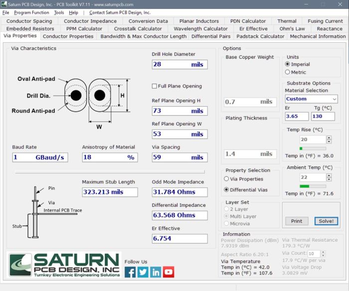
A simple 26 layer test vehicle was fabricated to compare the accuracy of the differential via circuit model to real vias. It consisted of two differential via pairs separated by 6 inches of 100 Ohm stripline differential pairs. Three sample via structures representing long, medium and short via stubs, as summarized in Figure 6, were measured using an Agilent N5230A VNA.
The differential vias had the following common parameters:
 Via drill diameter; D = 28 mils
Center to center pitch; s = 59 mils
Oval anti-pads= 53 mils x 73 mils
Dk of the laminate = 3.65
Anisotropy in Dkxy = 18%
Zvia = Zstub = 31.7 Ohms (per Equation 1)
Dkeff = 6.8 (per Equation 2)
Agilent ADS software was used to model and facilitate simulation correlation of the measured data as captured in Figure 7. This simple model accounts for the discontinuity of the long through section and the long stub section. The top half is the measured channel using an S-parameter file. The bottom half is a circuit model of the channel. Since the probes were not calibrated out, they are part of the device under test. The balun transformers are used to facilitate the display of the S-parameter and TDR results.
The comparison between the measured and simulated results of the insertion loss and TDR response for the three via stub cases using this simple approximation methodology is summarized in Figure 8. The insertion loss plots, in the frequency domain, are shown on the left, while the TDR plots are shown on the right.
The resonant nulls in the SDD21 plots are due to the stub lengths. As you can see, the longer the stub, the lower the resonant frequency null. If this null happens at the Nyquist frequency of the bit rate, the eye will be totally closed. This is why we back-drill them out after the board has been fabricated.
The simulation correlation is excellent up to about 12 GHz. The TDR plots show excellent impedance matching and delay for all three cases, while the simulated stub resonant frequencies match the measured frequencies very well. As you can see, these simple approximations for Dkeff and Zvia are perfectly adequate in providing a quick and accurate circuit model for differential through hole vias typically used in backplane applications.
Summary:
As illustrated, a simple twin-rod model (Figure 2) is used as the basis for a practical differential via circuit modeling methodology. By using Equation 1 and Equation 2, you can quickly determine the odd-mode impedance and effective dielectric constant needed for the circuit model.
Of course, you should use this methodology first as a rough starting point to quickly estimate the performance of your differential via design. If your worst case topology simulations show the performance is marginal, then it is worth while to invest the time and money to develop a 3D full wave model to perform a more accurate analysis.
On the other hand, if you find this approximation shows the vias have little impact on the channel performance, it may be of greater value for you to invest your time and money in resolving other critical issues with your design.
Try it the next time you are losing sleep over your design challenges.
For more Information:
If you liked this design note and want to learn more, or get more details on this innovative via modeling methodology, you can visit my web site, LAMSIM Enterprises.com , and download a copy of the white paper I wrote along with Eric Bogatin and Yazi Cao titled, “Method of Modeling Differential Vias” .
While you are there, feel free to investigate my other white papers and publications.
If you would like more information on our signal integrity and backplane services, or how we can help you achieve your next high-speed design challenge, email us at: info@lamsimenterprises.com.
UPDATE: In collaboration with Saturn PCB, I am pleased to announce my differential via equations above have been incorporated in a new impedance calculator available now in Saturn PCB Tool Kit software suite.
Via Stub Termination -Brought to You by “The Stubinator”
Thick backplanes with long via stubs will cause unwanted resonances in the channel insertion loss compared to vias with little or no stub length as shown by the red and green traces in the plot of Figure 1. If these resonances occur at or near the Nyquist frequency of the bit rate, there will be little or no eye-opening left at the receiver.

Figure 1 Topology circuit model of 2 differential vias with 30 inches of PCB etch. Insertion loss plot of Long via-no stub (green); short via-long stub (red); stub terminated (blue). Received eye diagrams after optimized FFE receive equalization at 10GB/s. Modeled and simulated using Agilent ADS.
In a typical backplane application, the signal entering the via structure from the top will travel along the through portion until it reaches the junction of the internal track and stub. At that point, the signal splits with some of the signal continuing along the trace, and the rest continuing along the stub. If the signal was Arnold Schwarzenegger, he would say, “I’ll be back!”. Having done this gig before, he knows that when he reaches the end of the stub it’s like hitting a brick wall; there’s no where to go but back up the stub. Like Arnold, when the signal reaches the end of the stub, it reflects back up the stub. When it arrives at the same junction, a portion combines with the original signal and the rest continues back toward the source. If the round trip delay is half a cycle, the two waves are completely 180 degrees out of phase and there is cancellation of the original signal. The frequency where maximum cancellation occurs is called the ¼ wave resonant frequency, fo. Resonance nulls due to stubs in an insertion loss plot, like the one shown in Figure 1, occurs at the fundamental frequency fo and at every odd harmonic.
If you know the length of the stub (in inches) and the effective dielectric constant Dkeff, the resonant frequency can be predicted with the following formula:

(1)
It is common practice to reduce stub lengths in high-speed backplane designs by back-drilling the stubs as close as possible to the active internal signal layer. This is a complex and costly process involving setting individual drill depths on a per board basis. Special design features must be designed into the artwork to set correct back-drill depth. Furthermore, it is difficult to verify ALL back-drilled holes were drilled correctly. I know of a case where a backplane came back and one via (that they knew of) had a significantly longer stub than was specified. The problem showed up by accident when they were characterizing the channel using a VNA and saw an unexpected resonant null in the SDD21 insertion loss plot. When all was said and done, it turned out there was a glitch in the fabricator’s software controlling the back-drilling process. There is no practical way to find these faults; short of doing VNA measurements on 100% of the back-drilled holes. With hundreds of them in a typical high-speed backplane, the cost would be prohibitive. Thus we have to trust the fabrication process of the vendor(s).
If only there was a way to terminate the stub and get rid of all this back-drilling. Well there just might be a solution. After returning from last year’s DesignCon2010, I was intrigued by a paper presented by Dr. Nicholas Biunno on a new matched terminated stub technology developed by Sanmina-SCI Corporation. They call this technology MTSviaTM and it allows the embedding of metal thin-film or polymer thick film resistors within a PCB stack-up during its fabrication. I like to call it “The Stubinator”. They developed this technology as an alternative to back-drilling. The beauty of this is you can terminate all the high-speed via stubs on just one resistive layer at the bottom of the PCB.
Of course, for this to work, we need to terminate the vias with a resistance equal to the differential via impedance to be most effective. But how do we determine the via differential impedance without going through a bunch of trial and error builds? In a DesignCon2009 paper titled, “Practical Analysis of Backplane Vias” I coauthored with Eric Bogatin from Bogatin Enterprises L.L.C., Sanjeev Gupta and Mike Resso from Agilent Technologies, we showed how you can model and simulate differential vias as simple twin-rod transmission line structures using simple transmission line circuit models as shown in Figure 1. You can download a copy of this award-winning paper from my web site at: Lamsimenterprises.com .
After determining fo (either by measurement of a real structure or through 3D modeling) and solving for Dkeff by rearranging equation (1), the differential via impedance calculated using the following equation:

(2)
Where:
s = the center to center spacing of the vias
D = Drill diameter.
Example:
The differential vias used in the model of Figure 1 has the following parameters:
s = 0.059 in.
D = 0.028 in.
stub_length = 0.269 in.
Dkeff = 6.14 by Equation (1) and fo=4.4GHz ;
Zdiff = 66 Ohms by Equation (2).
By adding a 66 Ohm resistor across the bottom of each via stub in the model, the blue trace in the plot shows the stub resonance has completely disappeared at the expense of an additional flat loss of about -10dB. The eye has opened up nicely.
This “Stubinator” technology looks like it could be a promising alternative to back-drilling. It resolves many of the issues and limitations highlighted above. Combined with silicon that can accommodate the additional signal loading, it may extend the life of traditional copper interconnections for next generation of Ethernet standards beyond 10GB/s.
Fiber Weave Effect Timing Skew
 Fiber weave effect timing skew is becoming more of an issue as bit rates continue to soar upwards. For signaling rates of 5GB/s and beyond, it can actually ruin your day. For example, the figure on the left shows a 5GB/s received eye is totally closed due to 12.7 inches of fiber weave effect. It was modeled and simulated using Agilent ADS software.
So what is fiber weave effect anyways and why should we be concerned about it? Well, it’s the term commonly used when we want to describe the situation where a fiberglass reinforced dielectric substrate causes timing skew between two or more transmission lines of the same length. Since the dielectric material used in the PCB fabrication process is made up of fiberglass yarns woven into cloth and impregnated with epoxy resin, it becomes non-homogeneous.
 The speed at which a signal propagates along a transmission line depends on the surrounding material’s relative permittivity (er), or dielectric constant (Dk). The higher the Dk, the slower the signal propagates along the transmission line. When one trace happens to line up over a bundle of glass yarns for a portion of its length, as illustrated by the top trace in the figure on the left, the propagation delay is different compared to another trace of the same length which lines up over mostly resin. This is known as timing or phase skew and is due to the delta Dk surrounding the respective traces.
Fiber weave effect is a statistical problem. It is not uncommon for PCB designs to have long parallel lengths of track routing without any bends or jogs. This is particularly true in large passive backplane designs. Because the fiber weave pattern tends to run parallel to the x-y axis, any traces running the same way will eventually encounter a situation of worst case timing skew if you build enough boards. This was demonstrated by Intel after compiling more than 58,000 TDR and TDT measurements over two years. In 2007, Jeff Loyer et al presented a DesignCon paper “Fiber Weave Effect: Practical Impact Analysis and Mitigation Strategies” where they published the data and proposed techniques to mitigate the effect of fiber weave skew. They showed statistically it is possible to have a worst case timing skew of approximately 16ps per inch representing a delta Dk of approximately 0.8.
In high speed differential signalling this is an issue because any timing skew between the positive (D+) and negative (D-) data converts some of the differential signal into a common signal component. Ultimately this results in eye closure at the receiver and contributes to EMI radiation.
You can calculate the timing skew using the following equation:

Where:
tskew = total timing skew due to fiber weave effect length (sec)
Dkmax= dielectric constant of material predominated by fiberglass.
Dkmin= dielectric constant of material predominated by resin.
c = speed of light = 2.998E+8 m/s (1.18E+10 in/s)
 A practical methodology you can use to estimate the minimum and maximum values of Dk is by studying the material properties available from PCB laminate suppliers. Consider two extreme styles of fiberglass cloths used in modern PCB laminate construction as illustrated by the figure on the left. The loose weave pattern of 106 has the highest resin content of all the most popular weaves, while the tight weave pattern of 7628 has the lowest. Therefore, you could use the specified values of Dk for cloth styles 106 and 7628 to get Dkmin and Dkmax respectively. Once you have these and apply a tolerance, you can estimate the tskew .
Example:
Assume Fr4 material; one inch of fiber weave effect; Dk106= 3.34(+/-0.05) and Dk7628= 3.97(+/-0.05), then timing skew is calculated as follows:

Modern serial link interfaces use differential signalling on a pair of transmission lines of equal length for interconnect between two points. In a DesignCon 2007 paper, “Losses Induced by Asymmetry in Differential Transmission Lines” by Gustavo Blando et al, they showed how intra-pair timing skew between the positive (D+) and negative (D-) data caused an increase in the differential insertion loss profile due to timing induced resonances. These resonances appear as dips in the differential insertion loss profiles of the channel as shown in the following figure:

This figure presents the results from an ADS simulation I did recently of a PCIe Gen2 channel running at 5GT/s. The eye diagrams are at the receiver after approximately 30” of track length chip to chip. The channel model was parameterized to allow for adjusting the fiber weave effect length as required.
As you can see, when the length of the fiber weave effect induced skew increases from 0 to 12.7 inches, the fundamental frequency nulls in the differential insertion loss plots decrease. These nulls occur at the fundamental frequency (fo) and every odd harmonic.
Also, the eye shows some degradation at 5.6 inches of fiber weave effect and starts to distort significantly after 7.8 inches. At 12.7 inches, fo equals the Nyquist frequency of the data rate (in this case 2.5GHz) and the eye is totally closed.
You can predict the resonant frequency ahead of time and use it to gain some intuition before you simulate and validate the results. If you know the total intra-pair timing skew, fo is calculated using the following equation:
![]()
Where:
fo = resonant frequency
tskew = total intra-pair timing skew
Example:
Using tskew = 16 ps/in we calculated above and using 12.7 inches from the last simulation results in the figure above, the fundamental resonant frequency null is:

You can find more details of this phenomena plus a novel way to model and simulate it from a recent White Paper I published titled, “Practical Fiber Weave Effect Modeling”. It, along with other papers, is found on my website at LamsimEnterprises.com.
Characteristic Impedance and Propagation Delay of a Transmission Line
A transmission line is any two conductors with some length separated by a dielectric material. One conductor is the signal path and the other is its return path. As the leading edge of a signal propagates down a transmission line, the electric field strength between two oppositely charged conductors creates a voltage between them. Likewise, the current passing through them produces a corresponding magnetic field. A uniform transmission line terminated in its characteristic impedance will have a constant ratio of voltage to current at a given frequency at every point on the line.
To ensure good signal integrity, it is important to maintain a constant impedance at every point along the way. Any change in the characteristic impedance results in reflections which manifests itself into noise on the signal. In any printed circuit board design, it is almost impossible to maintain a constant impedance of the transmission path from transmitter to receiver. Things like vias, non-homogeneous dielectric, thickness variation and other component paracitics all contribute to impedance mismatch. In high-speed designs, uncontrolled impedance can significantly reduce voltage and timing margins to the point where the circuit may be marginal or worst inoperable. The best you can do is to try to minimize each impedance discontinuity when they occur.
Lossy Transmission Line Circuit Model:
 The circuit model for a lossy transmission line assumes an infinite series of two-port components as illustrated. The series resistor represents the distributed resistance with the units as ohms (Ω) per unit length. The series inductor represents the distributed loop inductance with the units as henries (H) per unit length. Separating the two conductors is the dielectric material represented by conductance G in siemens (S) per unit length. Finally, the shunt capacitor represents the distributed capacitance between the two conductors with units of farads (F) per unit length.
A 2D field solver is the best tool to extract these parameters from a given transmission line geometry. It assumes, however, that the same geometry is maintained through its entire length. Many spice like simulators need these RLGC parameters for their lossy transmission line models.
Given the RLGC parameters, the characteristic impedance can be calculated by the following equation:
![]()
Where:
Zo is the intrinsic characteristic impedance of the transmission line.
Ro is the intrinsic series resistance per unit length of the transmission line.
Lo is the intrinsic loop inductance per unit length of the transmission line.
Go is the intrinsic conductance per unit length of the transmission line.
Co is the intrinsic capacitance per unit length of the transmission line.
Lossless Transmission Line:
For the lossless transmission line model, Ro and Go are assumed to be zero. As a result, the equation reduces to simply:
![]()
Propagation Delay:
Propagation delay, as it relates to transmission lines, is the length of time it takes for the signal to propagate through the conductor from on point to another. Given the inductance and capacitance per unit length, the propagation delay of the signal can be determined by the following equation:
![]()
Where:
tpd is the propagation delay in seconds/unit length.
Lo is the intrinsic loop inductance per unit length of the transmission line.
Co is the intrinsic capacitance per unit length of the transmission line.
Relative permittivity is also known as relative dielectric constant . The number is a measure of an insulator material’s ability to transmit an electric field compared to a vacuum, which is 1. For simplicity, it is usually referred to it as just the dielectric constant, Dk.
Electromagnetic signals propagate at the speed of light through free space. When these signals are surrounded by insulating material other than air or a vacuum, the propagation delay increases proportionally. You can determine the propagation delay with a known Dk by the following equation:
![]()
Where:
Dk is the dielectric constant of the material.
c is the speed of light in free space = 2.998E8 m/s or 1.180E10 in/s.
Driver’s Output Impedance From IBIS
In a recent post from the SI-list I subscribe to asks a question; “How do you find the driver impedance information from the IBIS file?” Most of the time we want this information so that we can explore mitigation techniques to control reflections caused by impedance discontinuities of the transmission path.
IBIS stands for Input/Output Buffer Information Specification and is controlled by the IBIS Open Forum organization. It is a device modeling technique used in simulation to provide a simple table based; non-proprietary buffer model derived from a real semi-conductor device. IBIS models can be used to characterize I/V output curves, rising/falling waveforms and pin parasitics of the device packaging.
 When a driver’s output impedance is not matched to the transmission line characteristic impedance (Zo), there are reflections which causes ringing at the receiver as shown by the red waveform in the figure on the left. Terminating the transmission line at the receiver using a pull-up or pull-down resistor to match Zo is one way to cure this. Although this approach works fine, it is not the preferred method because the resistor value would be in the 45-70 Ohm range to match the typical single-ended transmission line impedances found in modern PCB designs. Such a low resistance causes additional loading on the driver resulting in higher power dissipation.
A better method is to add a series resistor at the end of the driver to make up the difference in impedance. For example if the buffer’s output impedance is 20 Ohms driving a 50 Ohm transmission line, you would add a 30 Ohm resistor in series with the output.
Because the buffer is a semi-conductor, it’s output impedance could vary based on rising/falling edge transitions, manufacturing process (slow, typical, fast), and the load it is driving. Since IBIS models are ASCII based, you can simply use your favourite text editor to view and quickly estimate the output impedance when driving 50 Ohms using two of the four V-T waveform tables.
Here’s how:
The output impedance is often different for the rising edge compared to the falling edge. To determine the output impedance of a low to high transition you would use the pull-down [Rising Waveform]; R_fixture = 50; V_fixture = 0.000 table. A sample of what this table looks like is shown below:
[Rising Waveform]
R_fixture = 50.0000
V_fixture = 0.000
| time V(typ) V(min) V(max)
|
0.000S 0.000V 0.000V 0.000V
0.2000nS 0.000V 0.000V -1.7835uV
0.4000nS -1.1143mV -8.0018uV -7.8340mV
0.6000nS 0.1336V -5.4161mV 0.9354V
0.8000nS 1.1220V -12.5300mV 2.3940V
* * * *
* * * *
9.6000nS 2.5680V 2.1880V 2.7880V
9.8000nS 2.5680V 2.1880V 2.7880V
10.0000nS 2.5680V 2.1880V 2.7880V
 The first three lines of the table tells us that the rising waveform has a 50 Ohm resistor connected to the buffer output and pulled-down to 0V as shown by the equivalent circuit on the right.
The combination of the output impedance (Zs) and the 50 Ohm load forms a simple voltage divider network described by the following equation:
![]()
Where:
VO = Voltage at the output pin of the buffer
VDC = Supply voltage
Zs = Buffer impedance
Solving for Zs, we end up with the following equation:
![]()
If VDC is 3.3V, and VO is 2.568V using the typical voltage at 10 nS from the V-T table above, the output impedance for the rising edge into 50 Ohms is equal to 14.25 Ohms.
To determine the output impedance of a high to low transition you would use the pull-up [Falling Waveform]; table similar to the following example:
[Falling Waveform]
R_fixture = 50.0000
V_fixture = 3.3000
V_fixture_min = 3.0000
V_fixture_max = 3.4500
| time V(typ) V(min) V(max)
|
0.000S 3.3000V 3.0000V 3.4500V
0.2000nS 3.3000V 3.0000V 3.4500V
0.4000nS 3.2995V 3.0000V 3.4500V
* * * *
* * * *
9.4000nS 0.5598V 0.6824V 0.4812V
9.6000nS 0.5598V 0.6824V 0.4812V
9.8000nS 0.5598V 0.6824V 0.4812V
10.0000nS 0.5598V 0.6824V 0.4812V

This time, the table tells us the falling waveform has a 50 Ohm resistor connected to the buffer output and pulled-up to V_fixture as shown by the equivalent circuit on the right.
The output impedance is calculated by the following equation:
![]()
Where:
VO = Output voltage when the driver is sinking current
V_Fix = Voltage of the test fixture
Using typical values for V_Fix = 3.3V and VO = 0.5598V at 10nS, Zs = 10.21 Ohms.
As you can see for this particular IBIS model, the output impedance varies depending on the edge transition. For a rising edge, the output impedance is 14.25 ohms and 10.21 Ohms for a falling edge when using the typical values. The impedances will also vary under min/max conditions.
If your load is something other than 50 Ohms, you should NOT rely on this simple method for signoff. Instead you should simulate it if the design is critical. Sometimes though we need a quick ball park number to gain some insight of a particular design or to give us some intuition of what to expect from simulation.
You can validate this methodology using any Spice-like simulator which supports IBIS models. There are many to choose from like HSPICE, Hyperlynx, Cadence Spectraquest, Ansoft Designer from ANSYS and Agilent ADS to name a few. Chances are if you work for a large company, you already have access to some of these tools. If you are a student or someone just starting to learn about signal integrity, there is an alternative available. Fortunately, Spectrum Software offers Micro-cap 10; a free trial of its SPICE software you can use. Although it is limited to the number of components, nodes and performance, it is more than adequate for this and other signal integrity studies. Personally, I found it quite easy to pick up and get productive fairly quickly.
 For the purpose of the analysis, the output buffer and it’s impedance (Zs) can be simplified as shown by the schematic on the left. When the buffer drives a 50 Ohm transmission line, you typically see the waveforms at the driver’s output (blue) and receiver’s input (red) as shown in the following plot:
 The initial step in the rising and falling edges of the blue waveform (Vs) is due to the voltage divider action between Zs and Zo. Let us call these steps as a “porch” and designate the voltages as Vp_rise/Vp_fall for the rising and falling porches respectively.
Vp_rise is equivalent to the maximum voltage of Rising Waveform table found in the IBIS model. Vp_fall is equivalent to the minimum voltage of Falling Waveform table.
The analysis is best summarized by the following Figure:

A common circuit topology was built using the schematic editor. The respective greyed-out devices are disabled during simulation making it a convenient way of switching them in and out for the different topologies. R1 is reserved for the series termination resistor and is set to 0 Ohms initially. Once the output impedance is determined, R1 is set to the difference between Zo and the output impedance Zs.
The top topology simulates the Pull-up test fixture and used to verify the Falling Waveform table in the IBIS model. Similarly, the center topology simulates the Pull-down test fixture for the Rising Waveform table. The bottom topology has the output buffer driving a real world 50 Ohm transmission line.
The results of the simulations are shown adjacent to their respective topologies. Referring to the last case, Vp_rise=2.555V and Vp_fall=3.3V-2.726V=0.574V . As you can see there is excellent correlation when you compare them against the IBIS model’s voltages of 2.568V and 0.5598V respectively. Using the simulated voltages and solving for Zs, we get 14.58 Ohms and 10.53 Ohms respectively.
Because Zs is different for the rise time and fall time, you can never perfectly compensate for the impedance mismatch. The best approach is sometimes to take the average value between the two. In this case Zs_avg=12.56 Ohms.
Once Zs is known, the series resistor can be calculated as follows:
![]()
When 38 ohms is substituted in the transmission line topology, the waveform is clean with minimum reflections as shown by the following results:

In conclusion, the methodology presented here is a simple and effective way to predict the driver’s output impedance from an IBIS model. Try it next time someone asks you the question, “How do you find the driver impedance information from the IBIS file?”
