Characteristic Impedance – Where SI/PI Worlds Collide
Originally published Signal Integrity Journal, February 23, 2021
Signal and power integrity (SI/PI) simulations, measurements, and analysis usually live in two different worlds, but occasionally these worlds collide. One such collision occurs when we refer to characteristic impedance, Z0. Traditionally the PI world lives in the frequency domain while the SI world lives in the time domain.
When designing a power distribution network (PDN) in the PI world, we are mostly interested in engineering a flat impedance below a target impedance from DC to the highest frequency components of the transient current. Practically this is achieved with a network of capacitors with different values connected to the respective power planes as shown in Figure 1.

Figure 1 A simplified model of a typical PDN courtesy [1].
In the real world, there is no such thing as an ideal capacitor. There are always parasitic elements known as equivalent series inductance (ESL) and equivalent series resistance (ESR). Physical characteristics of the PCB, like component mounting inductance, plane spreading inductance, via and BGA ball inductance, along with voltage regulator module (VRM) characteristics also contribute to the impedance profile. When connected together, the interaction of capacitors and parasitic inductance and resistance create a transfer impedance profile with resonant peaks and anti-resonant nulls as shown in Figure 2.
The transfer impedance between the VRM and the load is calculated and plotted in the frequency domain with a log-log scale. The resulted impedance curve is then compared to the target impedance (Ztarget), which is estimated based on the allowed noise ripple and maximum transient current. The flat target impedance is frequency independent in the analysis.

Figure 2 Impedance profile of the PDN as viewed from the pads on the die power rail courtesy [1].
Resonant peaks are due to ESL of one capacitor connected in parallel with another capacitor. Anti-resonant nulls are due to the series combination of ESR, ESL, and C for each capacitor. Different capacitor values will have anti-resonant nulls at different frequencies.
But in the PI world, there is a rarely talked about characteristic impedance, Z0. In this case, it refers to the geometric average of the reactive impedance of a capacitor (XC) and reactive impedance of an inductor (XL).
Equation 1

At resonance, XL and XC intersect at the characteristic impedance and are equal as shown in Figure 3.

Figure 3 Inductive and capacitive reactance plot of ideal inductor and capacitor versus frequency. At resonance, XL and XC are equal and intersect at the characteristic impedance, Z0. Simulated with Pathwave ADS [6].
This is a very important observation, and it is where the SI/PI worlds collide.
In the SI world, characteristic impedance, Z0 refers to the instantaneous ratio of the voltage to current of a wave front traveling along a uniform transmission line without reflections. For an infinitely long uniform transmission line, Z0 equals the input impedance.
The characteristic impedance of a lossy transmission line is defined as:
Equation 2

Where R is resistance per unit length; G is conductance per unit length; L is inductance per unit length; and C is capacitance per unit length. For a lossless uniform transmission line, R and G are assumed to be zero and thus the characteristic impedance is reduced to:
Equation 3

Time Domain Reflectometer
In the SI world, we usually use a time domain reflectometer (TDR) to measure characteristic impedance, but more often than not, the measured impedance we get is not what we predicted with a 2D field solver. Many 2D field solvers used by most PCB FAB shops only calculate the lossless characteristic impedance of the cross-sectional geometry at a single frequency, defined by the dielectric constant (Dk). It has no input for conductor resistivity, dielectric loss, or how long the conductor(s) is.
So the issue is: we design the stackup, then do our SI modeling analysis based on stackup parameters and matching characteristic impedance. But the PCB FAB shop will often adjust the line width(s), over and above normal process variation, so that when measured, the impedance will fall within the specified tolerance, usually +/-10 percent.
Part of the problem lies with the method used to take the measurements. Most PCB FAB shops follow IPC-TM-650 Test Methods Manual [2]. But it has limitations because Z0 measured is derived and cannot be directly measured. The reason is the measurements include resistive and dielectric losses, up to the point where the measurement takes place along the TDR plot.
Resistive loss often results in a slow monotonic rise in the impedance profile, shown in the example TDR plot of Figure 4. IPC-TM-650 specifies a measurement zone between 30-70 percent to avoid probing induced ringing affecting the measurements. Most PCB FAB shops will measure an average impedance over this range, usually in the center region.
Depending on the linewidth, thickness and dielectric dissipation factor (Df), the slope of the monotonic rise will vary.

Figure 4 Example TDR plot showing slow monotonic rise in impedance due to resistive losses and IPC-TM-650 measurement zone.
The problem is that the IPC-TM-650 test method was last updated back in 2004, when higher dielectric loss, along with wider line widths and thicker copper weights, were used more often. A higher Df tends to compensate for resistive loss by flattening the slope as shown in Figure 5.
On the bottom left is a simulated TDR plot using a high loss dielectric with Df = 0.024. The right side has the exact same geometry properties except Df = 0.004. The average impedance, when measured at the 50 percent point, is 49.8 Ohms on the left side vs. 51.4 Ohms on the right side. We also confirm flatter slope for high loss material.
The actual characteristic impedance predicted by a Polar SI9000 2D field solver [5] in Figure 5 is 49 Ohms. For higher loss material, measuring within the measurement zone would pass without any issues. But for lower loss material, the resistive loss dominates and measuring within the measurement zone will give ~5 percent higher impedance reading compared to the higher loss material. The correct measurement point for Z0 is, in fact, the initial dip, equivalent to the field solver prediction. Depending on the tolerance specified, this may affect yield and cost.

Figure 5 Characteristic impedance prediction by Polar SI9000 2D field solver [5] (top). Simulated 2 inch TDR plots using a high loss dielectric (bottom left) vs. low loss dielectric with exactly the same geometry (bottm right). A higher Df compensates for higher resistive loss thereby flattening the curve. Simulated with Pathwave ADS [6].
Today, with the push to low loss dielectric and finer line widths with thinner copper weights, measuring the true transmission line characteristic impedance using a TDR becomes more challenging. This is even more so when measuring differential impedance, because a change in line width space geometry can have a more profound effect on measured differential impedance.
Using the first article build of a new design, as an example, let’s assume the correct characteristic impedance, when measured at the beginning of the slow monotonic rise of a TDR plot, is on the high end of nominal +10 percent tolerance. Let’s say it’s 54 Ohms. But because of the low loss dielectric and high resistive loss, the TDR measurement at the midpoint is now reading 5% higher at 57 Ohms. This would imply the impedance is now out of spec over nominal and the board would be scrapped.
The PCB fab shop will then go back and adjust the linewidth accordingly for the next build to bring the measurement within range to their measurement set up. Doing this effectively lowers the true nominal characteristic impedance!
If subsequent manufacturing variations pushes the measured impedance within the measurement zone on the low end of the -10 percent tolerance, say 44 Ohms, then the true characteristic impedance, if measured at the initial dip, will be 5 percent lower at 42 Ohms and be out of spec. But the board will pass because it was measured following IPC-TM-650 test method.
2-port Shunt Measurement
But what if there were another way? What if we could borrow impedance measuring techniques from the PI world to determine the true transmission line characteristic impedance in the SI world? Well there is. Enter the 2-port shunt measurement technique.
For example, in the PI world, to measure ESL and ESR of a chip capacitor, of a device under test (DUT), a 2-port shunt measurement is often used. It is much like the 4-point Kelvin measurement technique used to measure very low DC resistance.
The 2-port shunt measurement is usually done with a 2-port vector network analyzer (VNA). Port 1 of the VNA sends out a calibrated signal, and port 2 measures the voltage signal across the DUT. Often an isolation transformer is also used to break the inherent ground loop when measuring ultra-low impedances [3].
Once the measurements have been completed and S-parameters saved in touchstone format, further analysis can be done in your favorite SPICE simulator. Figure 6 is a generic schematic using popular Pathwave ADS [5] that can be used for 2-port shunt analysis.
When port 1 and port 2 are connected to port 1 of the DUT and port 2 of the DUT is grounded, the impedance of the DUT can be determined by [3];
Equation 4


Figure 6 Generic Pathwave ADS [6] schematic used for 2-port shunt analysis on a S2P file for DUT.
If we replace the DUT in Figure 6 with a capacitor and inductor, we get an impedance plot shown in Figure 7. As we saw earlier, when we take the geometric average of the inductive and capacitive reactance using Equation 1, we get the characteristic impedance. If we apply Equation 4 to the results of a 2-port shunt measurements of a capacitor and inductor, we get exactly the same results as shown in the top of Figure 7.
When we replace the capacitor and inductor with a S-parameter file of a transmission line model from Figure 5, we get the plot shown at the bottom of Figure 7. Except for the resonant nulls and peaks, up to a certain frequency, the impedance of a transmission line looks like the impedance of a capacitor when the far-end is open, and looks like the impedance of an inductor when the far-end is shorted. And because of that, this is where the two worlds collide!
If we take the geometric average of the impedance when the far-end is open (Zopen) or shorted (Zshort), we get the characteristic impedance at that frequency. We note where the red and blue impedance lines first intersect, is exactly the geometric average characteristic impedance at that frequency.
Also worth noting, the lines intersect at half of the frequency between the peaks and valleys at higher frequencies as well.

Figure 7 Impedance of inductive and capacitive reactance vs. frequency (top) and impedance of a transmission line vs. frequency (bottom) when the far-end is open (solid red) compared to when the far-end is shorted (solid blue). The intersection of the red and blue lines is exactly the characteristic impedance. Simulated with Pathwave ADS [5].
We can see this more clearly if we replot Figure 7 bottom using a linear scale for the x-axis, as shown in Figure 8. This is a very powerful observation. What this means is that when we measure the impedance half way between a peak and adjacent valley, of either the red or blue plot, it is the characteristic impedance of the transmission line at that frequency.
Thus, only an open or shorted end measurement is all that is needed to determine the characteristic impedance. For example, if we look at the red curve alone, then measure the first resonant null (m14) and adjacent peak (m15), the characteristic impedance (mag(Zopen) is measured exactly at one half the frequency between the two (m16).

Figure 8 Impedance of a transmission line vs. frequency on a linear scale when the far-end is open (solid red) compared to when the far-end is shorted (solid blue). The intersection of the red and blue lines half way between respective peaks and valleys is the characteristic impedance. Simulated with Pathwave ADS [6].
The first resonant red null and blue peak represent the quarter-wave resonant frequency due to open and shorted end. Each respective red null and blue peak following are the odd harmonics of the first quarter-wave resonant frequency.
Knowing this, we can now determine the phase or time delay (TD) of the transmission line as being one quarter of the period of the resonant frequency (f0).
Equation 5

Because resonant nulls and peaks occur at the resonant frequency, we can also determine the effective dielectric constant (Dkeff). Given the speed of light (c) = 11.8 in. per nanosecond, the length of the transmission line (len) in in. and quarter-wave resonant frequency (f0), Dkeff can be determined by:
Equation 6

CMP28 Case Study

Figure 9 Photo of a portion of CMP-28 test platform courtesy of Wildriver Technology [8] used for measurement validation.
To test the accuracy of this method, measured data from a CMP28 test platform, shown in Figure 9, was used for measurement validation. S-parameter (s2p) files from 2 inch and 8 inch single-ended stripline traces were provided as part of CMP-28 design kit courtesy of Wildriver Technologies [8]. The 6-inch transmission line segment S-parameter data was de-embedded courtesy of AtaiTec Corporation [9].
The characteristic impedance, based on trace geometry and stackup parameters, was modeled in Polar SI9000 [5]. Using Dk from data sheet tables @ 10GHz, and correcting for conductor roughness [10], the characteristic impedance predicted was 49.66 Ohms, as shown in Figure 10.

Figure 10 Polar SI9000 field-solver [5] characteristic impedance prediction of CMP28 trace geometry.
Touchstone S-parameter DUT files were connected with far-end open, shorted, and terminated as shown in Figure 11. The TDR plot, with far-end terminated, shows an impedance of 50.57 Ohms, when measured at the initial peak. Then it takes an immediate dip to approximately 50 Ohms before continuing with a slow monotonic rise with some ripples. If the DUT was a uniform trace, with connector discontinuity de-embedded, we would not see the initial peak followed by the dip. This signature strongly suggests that the DUT is not uniform and thus it is very difficult to determine the actual characteristic impedance using IPC-TM-650 test method alone.
But only after taking 2-port shunt measurements can we confirm the true characteristic impedance. As shown, Zoavg is 50.68 Ohms where the red and blue curves cross at 122.5 MHz, and confirms the true measurement point in the TDR plot is the initial peak. Both are about 1 Ohm higher compared with 2-D field solver results in Figure 10.
If the length of the transmission line simulated above is 6 in. and f0 =248.2 MHz, then TD = 1 ns and Dkeff = 3.92, using Equation 5 and Equation 6 respectively.

Figure 11 Measured results from a CMP28 test platform design kit, courtesy of Wildriver Technology [8].
But wait a minute. Why is Dkeff is higher than what was used in the 2-D field solver in Figure 10?
One reason is due to process variation of the material and fabrication. The actual Dkeff is determined by the final thickness of dielectric and the roughness of the copper, which also increases inductance affecting TD [10] [11]. But the main reason is Dk is frequency dependent and the value used in the field solver was at 10 GHz, based on laminate supplier’s Dk/Df tables.
Since TD, ultimately determines Dkeff, it does not represent the intrinsic property of the dielectric material. Because Dkeff varies with frequency, it was calculated at the first resonant null of 248.2 MHz, which is at a much lower frequency for Dk than the frequency originally used to select Dk in the field solver.
As can be seen in Figure 12, a simulated vs. measured 2-port shunt frequency plot, with far-end open and shorted, we get exactly the same information, compared to the traditional method used to validate characteristic impedance and Dkeff.
If we measure the 39th odd harmonic frequency (H) at 9.884GHz for the resonant null closest to 10GHz, equating to the value of Dk used in Polar Si9000 2D field solver, Dkeff can be calculated with Equation 7:
Equation 7

The bottom right plot of Figure 12, shows Dkeff simulated (blue) vs. measured (red). As we can see, the measured Dkeff at 248.7 MHz is 3.94; pretty much agreeing with our earlier calculation of 3.92 using Equation 6. Furthermore, when we compare Dkeff = 3.76 at 9.884 GHz, it agrees with our calculation for the 39th harmonic frequency from Equation 7. The reason there is still a slight difference in Dkeff is because the added delay due to inductance due to roughness [11] was not factored into the simulated model.
The bottom left is a TDR plot that shows measured impedance (red) vs. simulated (blue) over time. The marker at the beginning of the initial dip (m6) represents the characteristic impedance with highest frequency harmonics included in the incident step edge of TDR waveform. The marker at the end (m16) represents the impedance at twice the TD with high frequency harmonics attenuated due to dispersion of the lossy dielectric and resistance of trace length.
When we measure Zoavg_meas impedance of DUT at 9.884GHz, at the top plot of Figure 12, it agrees pretty well with the simulated and measured TDR plot at the initial step.

Figure 12 Comparison of PI world 2-port shunt measurement results for transmission line characteristic impedance and Dkeff compared to traditional SI world measurement results. Top plot is the 2-port shunt simulated vs. DUT impedance measurements at the fundamental and 39th harmonic frequencies. Bottom left is beginning and end impedance measurements on TDR plot. Bottom right measuring equivalent Dkeff at fundamental and 39th harmonic frequencies.
Summary and Conclusion
Sometimes, when SI and PI worlds collide, we get the best of both worlds. By borrowing a simple 2-port shunt impedance measuring technique from the PI world, we have another tool at our disposal to measure true characteristic impedance, TD, and effective Dk from a uniformly designed transmission line in the SI world. The advantage is, unlike a TDR measurement, measuring true characteristic impedance using 2-port shunt method is not influenced by resistive or dielectric losses.
References
-
L. Smith, S. Sandler, E. Bogatin, “Target Impedance Is Not Enough,” Signal Integrity Journal, Vol. 1, Issue 1, January 2019; URL: https://www.signalintegrityjournal.com/ext/resources/MEDIA-KIT-2019/January-2019-Print-Issue/SIJ-January-2019-Issue_eBook_-V2.pdf
-
IPC-TM-650 Test methods Manual, Number 2.5.5.7, “Characteristic Impedance of Lines on Printed Boards by TDR”, Rev. A, March, 2004
-
I. Novak, J. Millar, “Frequency-Domain Characterization of Power Distribution Networks,” Artech House, 685 Canton St., Norwood, MA, 02062, 2007.
-
Pathwave Advanced Design System (ADS) [computer software], Version 2021, URL: http://www.keysight.com/en/pc-1297113/advanced-design-system-ads?nid=-34346.0&cc=CA&lc=eng
-
Polar Instruments Si9000e [computer software], Version 2018, URL: https://www.polarinstruments.com/index.html
-
Keysight Pathwave Advanced Design System (ADS) [computer software], Version 2021, URL: http://www.keysight.com/en/pc-1297113/advanced-design-system-ads?cc=US&lc=eng.
-
E. Bogatin, “Bogatin’s Practical Guide to Transmission Line Design and Characterization for Signal Integrity”, Artech House, 685 Canton St., Norwood, MA, 02062, 2020
-
Wild River Technology LLC 8311 SW Charlotte Drive Beaverton, OR 97007. URL: https://wildrivertech.com/
-
AtaiTec Corporation, URL: http://ataitec.com/products/isd/
-
B. Simonovich, “A Practical Method to Model Effective Permittivity and Phase Delay Due to Conductor Surface Roughness“, DesignCon 2017 proceedings, Santa Clara CA.
-
V. Dmitriev-Zdorov, B. Simonovich, I. Kochikov, “A Causal Conductor Roughness Model and its Effect on Transmission Line Characteristics”, DesignCon 2018 proceedings, Santa Clara, CA.
-
I. Novak et al, “Determining PCB Trace Impedance by TDR: Challenges and Possible Solutions”, DesignCon 2013 proceedings, Santa Clara, CA.
-
S. Sandler, “Easy trick to measure plane impedance with VNA”, EDN Asia, 2014, URL: https://archive.ednasia.com/www.ednasia.com/STATIC/PDF/201410/EDNAOL_2014OCT21_TEST_TA_01.pdf%3FSOURCES=DOWNLOAD
Single-ended to Mixed-Mode Conversions
Originally published in Signal Integrity Journal Magazine, July 2020
Signal Integrity (SI) engineers almost always have to work with S-parameters. If you haven’t had to work with them yet, then chances are you will sometime in your SI career. As speed moves up in the double-digit GB/s regime, many industry standards are moving to serial link-based architectures and are using frequency domain compliance limits based on S-parameter measurements.
A vector network analyzer (VNA) is the test instrument of choice to measure S-parameters from a device under test (DUT). By definition, each S-parameter (Sij) is the ratio of the sine wave voltage coming out of a port to the sine wave voltage that was going in to a port (Equation 1). Each S-parameter is complex with a magnitude and a phase.

Suffice it to say, for mathematical reasons, the indexes refer to the port in which the voltages are coming or going. This is counter intuitive to our normal train of thought and is important to be cognisant of this relationship when working with S-parameters.
Single-ended S-parameters
Figure 1 shows an example of a 1-Port, 2-Port and 4-Port DUTs and their respective S-parameter matrices representing uniform transmission lines with respective port index labelling. Each S-parameter in the matrix are single-ended measurements from one port to another.
A 1-Port DUT has one S-parameter (S11) shown in red. It is the ratio of the voltage coming out of Port 1 to the voltage going into Port 1. As a measure of reflected energy out of Port 1, it is also known as return loss (RL)
A 2-Port DUT has 4 S-parameters shown in blue. S-parameters with the same index subscript numbers, i.e. S11, S22 are RL. S-parameters with alternate index subscript numbers, are a measure of transmitted energy and is the ratio of the voltage coming out of a Port to the voltage going into the opposite Port. It is also known as insertion loss (IL). For example, S12 is the ratio of the voltage coming out of Port 1 to the voltage going into Port 2, whereas S21 is the ratio of the voltage coming out of Port 2 to the voltage going into Port 1.

Figure 1 From left to right examples of 1-Port (Red), 2-Port (Blue), 4-Port (Black) DUTs and their respective S-parameter matrices.
A 4-Port DUT has 16 S-parameters, divided into 4 quadrants, shown in black. As you can see the number of S-parameter combinations is the square of the number of ports. In this example, the top left quadrant 1 and bottom right quadrant 4 are the same as individual 2-Port DUTs with different port indices. They are described as:
Quadrant 1:
-
S11 is the ratio of the voltage coming out of Port 1 to the voltage going into Port 1. It is the RL out of Port 1.
-
S12 is the IL and is the ratio of the voltage coming out of Port 1 to the voltage going into Port 2. It is the IL from Port 2 to Port 1.
-
S21 is the ratio of the voltage coming out of Port 2 to the voltage going into Port 1. It is the IL from Port 1 to Port 2. For a uniform transmission line, S21 = S12.
-
S22 is the ratio of the voltage coming out of Port 2 to the voltage going into Port 2. It is the RL out of Port 2. For a uniform transmission line, S22 = S11.
Quadrant 4:
-
S33 is the ratio of the voltage coming out of Port 3 to the voltage going into Port 3. It is the RL out of Port 3
-
S34 is the ratio of the voltage coming out of Port 3 to the voltage going into Port 4. It is the IL from Port 4 to Port 3
-
S43 is the ratio of the voltage coming out of Port 4 to the voltage going into Port 3. It is the IL from Port 3 to Port 4. For a uniform transmission line, S43 = S34.
-
S44 is the ratio of the voltage coming out of Port 4 to the voltage going into Port 4. It is the RL out of Port 4. For a uniform transmission line, S44 = S33
S-parameters in the top right quadrant 2 and bottom left quadrant 3 describe the near-end and far-end coupling of the respective ports. When unwanted coupling happens at the near-end, it is referred to as near-end cross talk, or NEXT. When it happens at the far-end, it is known as far-end crosstalk, or FEXT.
Quadrant 2:
-
S13 is the ratio of the voltage coming out of Port 1 to the voltage going into Port 3. It is the coupling or NEXT from Port 3 to Port 1.
-
S14 is the ratio of the voltage coming out of Port 1 to the voltage going into Port 4. It is coupling or FEXT from Port 4 to Port 1.
-
S23 is the ratio of the voltage coming out of Port 2 to the voltage going into Port 3. It is coupling or FEXT from Port 3 to Port 2.
-
S24 is the ratio of the voltage coming out of Port 2 to the voltage going into Port 4. It is coupling or NEXT from Port 4 to Port 2.
Quadrant 3:
-
S31 is the ratio of the voltage coming out of Port 3 to the voltage going into Port 1. It is the coupling or NEXT from Port 1 to Port 3.
-
S32 is the ratio of the voltage coming out of Port 3 to the voltage going into Port 2. It is coupling or FEXT from Port 2 to Port 3.
-
S41 is the ratio of the voltage coming out of Port 4 to the voltage going into Port 1. It is coupling or FEXT from Port 1 to Port 4.
-
S42 is the ratio of the voltage coming out of Port 4 to the voltage going into Port 2. It is coupling or NEXT from Port 2 to Port 4.
Although there is no industry standard for labeling a 4 or more port DUT, a practical way is to use the port order shown so that the 2-Port DUT is a subset of the top left quadrant of the 4-Port DUT. When you do this, the port order labeling is consistent as you increase the number of ports; with odd ports on the left and even ports on the right. S12 and S21 always describe the IL terms; while S13 and S31 define the NEXT terms.
But sometimes 3rd party 4-port S-parameters are labeled with ports 1 and 2 are on the left side, while ports 3 and 4 are on the right side. In this configuration, S31 and S42 are now the IL terms. This is counter intuitive when moving from 2-Port to 4 or more Port DUT and leading to potential confusion when cascading S-parameters to build a channel model, or converting to mixed-mode S-parameters. Whenever you get S-parameter files from 3rd party, it is always prudent to test it and compare IL plots against port order to ensure you are using them correctly.
Typically, 4-port S-parameters are saved in Touchstone format with a .snp extension, where n is the number of ports. Many Electronic Design Automation (EDA) and circuit simulation software tools allows you to view and plot S-parameters from Touchstone files.
Figure 2 is a schematic of a 4-port S-parameter component used in Keysight ADS. When the component is linked to appropriate .s4p touchstone file and ports connected as shown, the 16-port S-parameter matrix can be plotted and analyzed.

Figure 2 Keysight ADS schematic used to plot 4-Port single-ended S-parameters.
The 1-port and 2-port S-parameters are included in the same plot as the 4-port S-parameters plotted in Figure 3. The top left (red) and bottom right (green) quadrants plot the return loss (RL) and insertion loss (IL), while the top right (blue) and bottom left (magenta) quadrants plot the NEXT and FEXT.

Figure 3 An example of 4-Port S-parameter single-ended plots of a uniform transmission line.
Mixed-mode S-parameters
SI engineers often have to check channel models and S-parameter measurements against industry standard compliance plots. Many of those plots are in terms of mixed-mode S-parameters, which means the single-ended measurements need to be converted to mixed-mode matrix.
Two single-ended transmission lines with coupling are also known as a differential pair, as shown in Figure 4. When we talk about single-ended transmission lines with coupling, we are usually interested in their single-ended properties like characteristic impedance (Zo), phase delay, and NEXT/FEXT relationships as described above.
But when we talk about a differential pair, we are interested in the mixed-mode S-parameters like differential and common signals and how they interact within the pair. Because we are describing the exact same interconnect, they are equivalent.
When describing a differential pair, there are only four possible outcomes in response to an input signal as defined by the mixed-mode S-parameter matrix:
-
A differential signal enters the differential pair and a differential signal comes out
-
A differential signal enters the differential pair and a common signal comes out
-
A common signal enters the differential pair and a differential signal comes out
-
A common signal enters the differential pair and a common signal comes out

Figure 4 Single-ended vs mixed-mode S-parameter matrices of two coupled transmission lines.
Mixed-mode S-parameters in each quadrant are described as:
SDD Quadrant (Red):
-
SDD11 is the ratio of the differential signal coming out of Port 1 to the differential signal going into Port 1. It is the differential RL out of Port 1.
-
SDD12 is the ratio of the differential signal coming out of Port 1 to the differential signal going into Port 2. It is the differential IL from Port 2 to Port 1.
-
SDD21 is the ratio of the differential signal coming out of Port 2 to the differential signal going into Port 1. It is the differential IL from Port 1 to Port 2.
-
SDD22 is the ratio of the differential signal coming out of Port 2 to the differential signal going into Port 2. It is the differential RL out of Port 2.
SDC Quadrant (Blue):
-
SDC11 is the ratio of the differential signal coming out of Port 1 to the common signal going into Port 1.
-
SDC12 is the ratio of the differential signal coming out of Port 1 to the common signal going into Port 2.
-
SDC21 is the ratio of the differential signal coming out of Port 2 to the common signal going into Port 1.
-
SDC22 is the ratio of the differential signal coming out of Port 2 to the common signal going into Port 2.
SCD Quadrant (Magenta):
-
SCD11 is the ratio of the common signal coming out of Port 1 to the differential signal going into Port 1.
-
SCD12 is the ratio of the common signal coming out of Port 1 to the differential signal going into Port 2.
-
SCD21 is the ratio of the common signal coming out of Port 2 to the differential signal going into Port 1.
-
SCD22 is the ratio of the common signal coming out of Port 2 to the differential signal going into Port 2.
SCC Quadrant (Green):
-
SCC11 is the ratio of the common signal coming out of Port 1 to the common signal going into Port 1.
-
SCC12 is the ratio of the common signal coming out of Port 1 to the common signal going into Port 2.
-
SCC21 is the ratio of the common signal coming out of Port 2 to the common signal going into Port 1.
-
SCC22 is the ratio of the common signal coming out of Port 2 to the common signal going into Port 2.
Single-ended S-parameters, with port order shown in Figure 4, can be mathematically converted into mixed-mode S-parameters using equations shown in Table 1.

Alternatively, Keysight ADS can simplify this process using equations on 4-Port single-ended or using 4-port Balun components, as shown in Figure 5.

Figure 5 Keysight ADS schematic used to convert from 4-Port single-ended to 2-Port mixed-mode S-parameters using equations or 4-Port Balun components. Differential and common port numbering as D1, D2, C1, C2 respectively.
Figure 6 plots mixed-mode S-parameters from equations in Table 1. Each quadrant is color coded to coincide with the respective table quadrants.

Figure 6 An example of 4-Port S-parameter mixed-mode plots of a differential transmission line.
References:
[1] M. Resso, E. Bogatin, “Signal Integrity Characterization Techniques”, International Engineering Consortium, 300 West Adams Street, Suite 1210, Chicago, Illinois 60606-5114, USA, ISBN: 978-1-931695-93-0
https://www.amazon.com/Signal-Integrity-Characterization-Techniques-Bogatin-ebook/dp/B07P9277WY/ref=sr_1_fkmr0_1?keywords=bogaitn+resso&qid=1581289220&sr=8-1-fkmr0
[2] A. Huynh, M. Karlsson, S. Gong (2010). Mixed-Mode S-Parameters and Conversion Techniques, Advanced Microwave Circuits and Systems, Vitaliy Zhurbenko (Ed.), ISBN: 978-953-307-087-2,InTech, Available from: http://www.intechopen.com/books/advanced-microwave-circuits-and-systems/mixed-mode-s-parameters-and-conversion-techniques.
[3] Alfred P. Neves, Mike Resso, and Chun-Ting Wang Lee, “S-parameters: Signal Integrity Analysis in the Blink of an Eye”, Signal Integrity Journal, https://www.signalintegrityjournal.com/articles/432-s-parameters-signal-integrity-analysis-in-the-blink-of-an-eye
Keysight Advanced Design System (ADS) [computer software], (Version 2020). URL: http://www.keysight.com/en/pc-1297113/advanced-design-system-ads?cc=US&lc=eng.
Differential Impedance and Why We Care
Originally published in Signal Integrity Journal April 14,2020
What is Differential Impedance and Why do We Care?
Simply put, differential impedance is the instantaneous impedance of a pair of transmission lines when two complimentary signals are transmitted with opposite polarity. For a printed circuit board (PCB) this is a pair of traces, also known as a differential pair. We care about maintaining the same differential impedance for the same reason we care about maintaining the same instantaneous impedance of a single-ended (SE) transmission line: to avoid reflections.
There is really nothing special about differential pairs, other than maintaining the correct differential impedance. But you must understand the implications of the spacing between the traces in a pair.
The differential impedance is simply twice the odd-mode impedance of each trace. SE impedance is the impedance of a single trace and only equals the odd-mode impedance when there is little or no intra-pair coupling between them. When the traces are brought closer together, the differential impedance is reduced, unless the line widths are adjusted to compensate. (More about this later.)
Figure 1 shows the effect on intra-pair coupling of a pair of edge-coupled stripline traces driven differentially. The top figure shows electromagnetic fields surrounding a loosely coupled pair of traces 3.5 line-widths apart. The bottom figure shows a closely coupled pair at 1.5 line-widths apart. The red plus trace is current flowing into the page while the minus blue trace is current flowing out of the page.
The circular lines surrounding each trace are the magnetic fields representing loop inductance. The direction of rotation is based on current direction, using the right-hand rule. The electric field (e-field) lines are perpendicular to the magnetic field lines. They are a measure of capacitance.
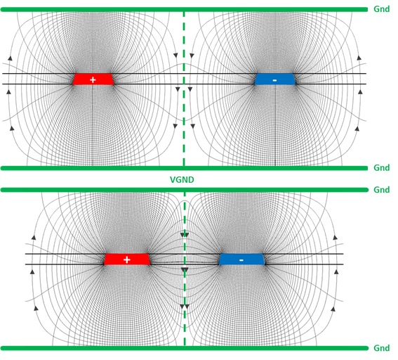
Figure 1. Effect on intra-pair coupling of a pair of edge-coupled stripline traces driven differentially. Top figure shows electromagnetic fields surrounding a loosely coupled pair of traces 3.5 line-widths apart. Bottom figure shows a closely coupled pair at 1.5 line-widths apart.
When the traces are loosely coupled, the electric and magnetic field lines are fairly symmetrical around each trace, and are mirror images of one another about the center line between them. Most of the respective e-field coupling is to the reference ground planes. As the traces are moved closer to one another, the counter-rotating rings compress about the centerline, lowering the inductance. At the same time, more of the e-field lines along the inside edge of each trace tend to couple to one another, increasing the capacitance.
Because of the way the EM-fields interact along the centerline, we can think of it as a virtual ground (VGND) reference plane. They behave exactly the same way as if there is a solid reference plane between them.
Odd-Mode Impedance
Consider a pair of equal width microstrip line traces, labeled 1 and 2, with a constant spacing between them as shown in Figure 2. Assuming lossless transmission lines, each individual trace, when driven in isolation, will have a SE characteristic impedance Zo, defined by the self-loop inductance (L11, L22) and self-capacitance (C11, C22) with respect to the GND reference plane.
When the pair of traces are driven differentially, the mode of propagation is odd. The electromagnetic field interaction is shown in Figure 1. When the intra-pair spacing is close, there will be electromagnetic coupling defined by the mutual inductance (Lm) and mutual capacitance (Cm).
The proximity of the traces to a reference plane influences the amount of electromagnetic coupling between traces. The closer the traces are to the reference plane, the lower the self-loop inductance and stronger self-capacitance; resulting in a lower mutual inductance, and weaker mutual capacitance between traces. The end result is a lower differential impedance.
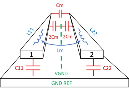
Figure 2. Pair of microstrip traces showing self-loop inductance (L11, L22), self-capacitance (C11, C22), mutual capacitance (Cm) and mutual inductance (Lm) when line 1 and line 2 are driven differentially.
A 2D field solver is usually used to extract the parameters for a given geometry. Once the resistance, inductance, conductance, and capacitance (RLGC) parameters are extracted, an L C matrix can be set up as follows:
L11 L12 C11 C12
L21 L22 C21 C22
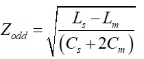
The self-loop inductance and self-capacitance for trace 1 and 2 are L11, C11, L22, C22 respectively. In a perfectly symmetrical differential pair, the off-diagonal (12, 21) terms in each matrix are the mutual inductance and mutual capacitance respectively. The LC matrix can be used to determine the odd-mode impedance. It can be calculated by the following equation [1]:
Equation 1
Where:
Zodd = odd mode impedance
Ls = self-loop inductance = L11 = L22
Cs = self-capacitance = C11 = C22
Lm = mutual inductance = L12 = L21
Cm = mutual capacitance = |C12 |=|C21|
Example
A Polar SI9000 field solver is used to compare a loosely coupled pair, with 4 mil traces, separated by 20 mil space, vs. a SE transmission line with the same dielectric thickness (see Figure 3). The LC matrix was extracted at 10GHz. As can be seen, the odd-mode impedance of the loosely coupled pair equals the characteristic impedance of the SE trace, and thus differential impedance would be the same.
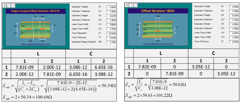
Figure 3. Comparison of a loosely coupled pair (left), with 4 mil traces, separated by 20 mil space, vs. a SE transmission line (right) with the same dielectric thickness. Odd-mode impedance of the loosely coupled pair equals the characteristic impedance of the SE trace.
But if you route a pair of traces with close coupling, the odd-mode impedance is less than the SE impedance for the same trace width (unless you adjust the line width). For example, on the left side of Figure 4, a 4-4-4 mil geometry has a differential impedance of 91 Ohms. In order to get 100 Ohms differential, the line width must be reduced to 3.35 mils and space adjusted to 4.65 mils to keep the same 12 mil center-center pitch, shown on right.

Figure 4. Comparison of 4-4-4 mil geometry (left) vs. 3.35-4.65-3.35 geometry (right) to achieve 100 Ohm differential impedance for the same center-center pitch.
But it doesn’t end there.
For some industry standards, there is usually a very short reach (VSR) spec which has a maximum channel loss defined. For example, the IEEE 802.3 CAUI-4 chip-module (C2M) spec budgets 7.5 dB at 12.89 GHz Nyquist frequency from the chip’s pins to a faceplate module’s pins, e.g. small form-factor pluggable (SFP) module. Because of modern top-of-rack routers and switches, it is not unusual to have 10 or more inches between the main switch chip and SFP module, the differential pair geometry design becomes important to satisfy both differential impedance and insertion loss (IL).
Reduced line width and tighter coupling results in higher loss over the length of the channel. Using the above examples, differential IL is plotted in Figure 5 for all three differential pairs. Loose coupling is shown in green; tight coupling without line width adjustment (Tight1) is shown in red, while tight coupling with line width adjustment (Tight2) is shown in blue.
As you can see, there is about a half dB difference at 12.89 GHz between loose coupling and both tight coupling examples over 10.6 inches. Tight coupling increases IL, regardless if line width is adjusted to meet differential impedance. In this example, there is only 0.1 dB delta between Tight1 and Tight2, which suggests most of the higher loss is due to tighter coupling.
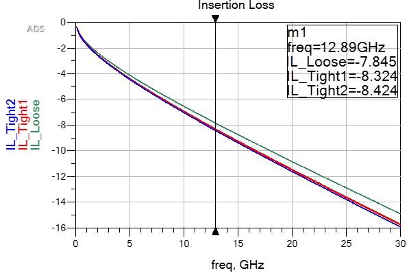
Figure 5. Differential IL comparison of loose coupling (green); Tight1 coupling without line width adjustments (red) and Tight2 coupling with line width adjustment (blue).
This can be explained by reviewing SE to differential mixed-mode conversion. Given a 4-port S-parameter, with SE port order as shown in Figure 6, the differential IL is determined by;
Equation 2
![]()
Where:
SDD21 = the differential IL defined by the ratio of the differential signaling coming out of port 2 to the differential signal going into port 1
S21 = the SE IL defined by the ratio of the SE signaling coming out of port 2 to the SE signal going into port 1
S43 = the SE IL defined by the ratio of the SE signaling coming out of port 4 to the SE signal going into port 3
S23 = far-end crosstalk coupling from port 3 to port 2
S41 = far-end crosstalk coupling from port 1 to port 4
As you can see from Equation 2, when the traces get closer together, and the coupling terms get larger, differential IL increases.
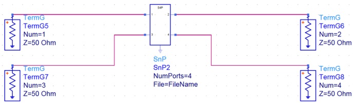
Figure 6. SE 4-port S-parameter port labeling.
Figure 7 plots differential TDR of all three examples. The steeper monotonic rise of the blue trace is due to higher resistive loss of 3.35 mil traces, as compared to the 4 mil traces in the other two examples.
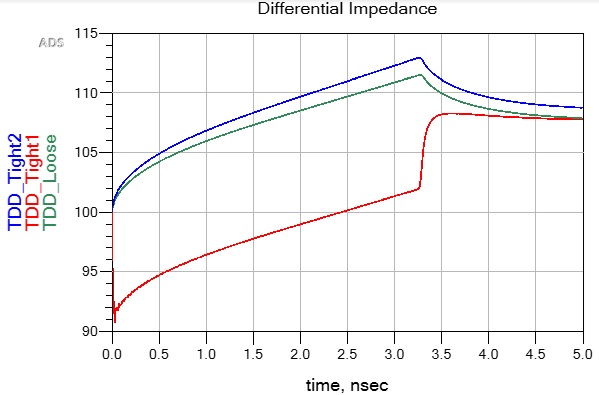
Figure 7. Differential TDR comparison of loose coupling (green); Tight1 coupling without line width adjustments (red) and Tight2 coupling with line width adjustment (blue).
To summarize then, it doesn’t matter if a differential pair is tightly coupled or loosely coupled. Properly engineered, both can be designed to properly match the output driver impedance. But as we have seen, each will have advantages and disadvantages.
Tighter coupling gives you better routing density at the expense of higher loss. Loose coupling allows for easier routing around obstacles and less loss. But in either case, they must be designed and measured for differential impedance.
So why is this important?
PCB fabrication shops use impedance as a metric to determine if the board has been fabricated to specification. Because the odd-mode impedance of a tightly spaced pair of traces depends on driving both traces differentially, you will not be able to determine the differential impedance by just measuring SE impedance of a tightly coupled pair like you could with two uncoupled traces.
References:
-
E. Bogatin, “Signal Integrity Simplified”, 3rd edition, Prentice Hall PTR, 2018
-
Keysight Advanced Design System (ADS) [computer software], (Version 2020)
-
Polar Instruments Si9000e [computer software] Version 2017
How Authorship Advances Your Career and Become an Industry Influencer
 So how can authorship advance your career and lead to becoming an industry influencer?
Well first of all, it offers a chance for deep learning of a subject matter. When you have to capture your thoughts on paper, you suddenly realize you may not know as much about the subject as you think you know. It forces you to do more research on the topic so that the information you are trying to covey is accurate.
It demonstrates thought leadership at your work and the industry. You become the subject matter expert on that topic. And over time, the path to your desk, is worn from all the traffic to your cubicle. If you are self employed as a consultant, it eventually leads to more business opportunities.
It inspires your coworkers and peers to become subject matter experts in their own right by leading by example. Being a subject matter expert offers opportunities to work with other subject matter experts in your company on leading edge projects.
It builds your personal brand. By writing papers and presenting at conferences you become known in the industry from the work you have accomplished and shared.
It gives you a chance to network, meet and collaborate with new people with like interests in the industry. It’s a snowball effect. I can’t even begin to count now many new people from around the world I have met since starting to publish and attend conferences.
It builds self confidence. Everyone at one time or another has had a fear of public speaking. By presenting your work in an audience of your peers, that fear of public speaking begins to dissipate.
Personal pride. Just like a “runner’s high”, you get a dopamine hit every time you see your work published or you present. There is no greater feeling, after spending an enormous amount of time writing your paper, making your slides perfect, continually practicing your presentation, to anyone who will listen, then finally delivering to an audience. It becomes addictive so you will want to continually publish and present your work.
It leaves a lasting legacy of part of your life’s work behind. Let’s face it, our time is limited on this earth. By publishing your work, it inspires future generations in their research, just like past generations of authors have inspired many of today’s authors, including myself.
You don’t have to start big. A personal blog, web site is a good place to begin. Trade journals, and online magazines in your industry are always looking for quality content that is relevant to their readers.
Formal societies, like IEEE, is a more recognized venue and is peer reviewed. Submitting a paper to industry conferences is another way and offers the opportunity to present your work. And finally, the ultimate, is publishing a book.
Once your work is published, then you need to self promote what you have done. Use social media like LinkedIn, Facebook, Twitter or any other platform. You eventually will build a following, who will react and share your posts and soon become an industry influencer.
Finally, I’d like to leave you with this final thought. Being Canadian, our national pastime is Hockey. We usually have a hockey analogy for almost anything. Everyone who follows hockey knows Wayne Gretzky, the greatest hockey player of all time. One of his famous quotes was, “You always miss 100% of the shots you don’t take.” And likewise, if you do not take the shot of writing a paper, book or an article, you cannot become a subject matter expert or industry influencer.
Go for it!
Simonovich-Cannonball Conductor Roughness Model Demystified
Recently on the SI-List there was great debate on whether or not my Cannonball model can be used to determine surface ratio and radius of sphere parameters needed for Huray roughness model from data sheets alone.
The author of this paper, “Conductor surface roughness modeling: From “snowballs” to “cannonballs”, [1] argues it is impossible to accurately model transmission lines from data sheets alone and seems to imply that because I had measured data in advance that I had magically “adjusted” Rz parameter to get such good correlation to measurements in my EDICon 2016 paper, “Practical Model of Conductor Surface Roughness Using Cubic Close-packing of Equal Spheres” [5].
Unfortunately his paper has created more confusion than clarity. To be clear, there is only ONE “Cannonball” model, and it is based on the cubic close packing of equal spheres, also known as face-centered cubic (FCC) packing.
The author of [1] also advocates using a material model identification methodology, similar to what I like to call the Design Feedback Method, shown in Figure 1. The author believes it is the only “accurate” way of determining printed circuit board (PCB) material properties for modeling.

Figure 1 Design Feed Back Method flow chart
This involves designing, building and measuring a test coupon with the intended PCB trace geometry to be used in final design. After modeling and tuning various parameters to best fit measured data, material parameters are extracted and then used in channel modeling software to design the final product.
The problem with this approach for many small companies is: TIME, RESOURCES, and MONEY.
-
Time to define stackup and test structures.
-
Time to actually design a test coupon.
-
Time to procure raw material – can take weeks, depending on scarcity of core/prepreg material.
-
Time to fabricate the bare PCB.
-
Time to assemble and measure.
-
Time to cross-section and measure parameters.
-
Time to model and fit parameters to measurements.
Then there is the issue of resources, which include having the right test equipment and trained personnel to get trusted measurements.
In the end this process ultimately costs more money, and material properties are only accurate for the sample from which they were extracted for the software and roughness model used. There is no guarantee extracted parameters reflect the true material properties.
There will be variation from sample to sample built from the same fab shop and more so from different fab shops because they have a different etch line and oxide alternative process.
For example Figure 2 shows measurements from two boards of the same design. As you can see there are differences in both insertion loss and TDR plots. Which curve do we use to fit parameters for material extraction to use in simulations? How many do we have to build and test to get a statistical sample of reality? How much time will this take? And how much money will it cost, especially if several PCB stackup geometries are required?

Figure 2 Comparison of insertion loss and TDR measurements of two boards of the same design
But, as Eric Bogatin often likes to say, “Sometimes an OK answer NOW is better than a good answer late”. For many signal integrity engineers, and design consultants, like myself, have to come up with an answer sooner, rather than later for many reasons. And depending on the issue at hand, those answers may be good enough. This was the initial motivation for my research.
So where do we get these parameters? Often the only sources are from manufacturers’ data sheets alone. But in most cases, the numbers do not translate directly into parameters needed for the EDA tools.
This paper will revisit the Cannonball model as it applies to the CMP-28 reference platform from Wildriver Technology [14], and as part of it I will show:
-
How to determine effective dielectric constant (Dkeff) due to roughness from data sheets alone.
-
How to apply my simple Cannonball stack model to determine roughness parameters needed for Huray model from data sheets alone.
-
How to apply these parameters using Simbeor software [10].
-
How to pull it all together with a simple case study.
But before we get into it, it is important to give a bit of background on material properties and PCB fabrication process.
Electro-deposited Copper
Electro-deposited (ED) copper is widely used in the PCB industry due to its low cost. A finished sheet of ED foil has a matte side and drum side. The matte side is usually treated with tiny nodules and is the side bonded to the core laminate. The drum side is always smoother than the matte side. For high frequency boards, sometimes the drum side of the foil is treated instead and bonded to the core. In this case it is known as reversed treated foil (RTF).
IPC-TM-650-2.2.17A defines the procedure for determining the roughness or profile of metallic foils used on PCBs. Profilometers are often used to quantify the roughness tooth profile of electro-deposited copper.
Nodule treated tooth profiles are typically reported in terms of 10-point mean roughness (Rz). Some manufacturers may also report root mean square (RMS) roughness (Rq). For standard foil this is the matte side. For RTF it is the drum side. Most often the untreated, or prepreg side, reports average roughness (Ra) in manufacturers’ data sheets.
With the realization of roughness having a detrimental effect on insertion loss (IL), copper suppliers began providing very low profile (VLP) and ultra-low profile (ULP) class of foils. VLP foils have treated roughness profiles less than 4 μm while ULP foils are less than 2 μm. Other names for ULP class are HVLP or eVLP, depending on the foil manufacturer.
It is important to obtain the actual vendor’s copper foil data sheet used by the respective laminate supplier for accurate modeling.
Oxide/Oxide Alternative Treatment
In order to promote good adhesion of copper to the prepreg material during the PCB lamination process, the copper surface is treated with chemicals to form a thin, nonconductive film of black or brown oxide. The controlled oxidation process increases the surface area, which provides a better bond between the prepreg and the copper surface. It also passivates the copper surface to protect it from contamination.
Although oxide treatment has been used for many years, eventually the industry learned that the lack of chemical resistance resulted in pink ring, which is indicative of poor adhesion between copper and prepreg. This weakness has led to oxide alternative (OA) treatments which rely on some sort of etching process, but no oxide layer is formed.
With the push for smoother copper to reduce conductor loss, newer chemical bond enhancement treatments, working at the molecular level, were developed to maintain copper smoothness, yet still provide good bonding to the prepreg.
Since OA treatment is applied to the drum side of the foil during the PCB Fabrication process, the OA roughness numbers should be used instead of Ra specified in foil manufacturer’s data sheets. RTF foil is modeled differently and discussed later in the case study.
Tale of Two Data Sheets
Everyone involved in the design and manufacture of PCBs knows the most important properties of the dielectric material are the dielectric constant (Dk) and dissipation factor (Df ).
Using Dk / Df numbers for stackup design and channel modeling from “Marketing” data sheets, like the example shown in Figure 3, will give inaccurate results. These data sheets are easily obtained when searching laminate supplier’s web sites.

Figure 3 Example of a “Marketing” data sheet easily obtained from laminate supplier’s web site. Source Isola Group.
Instead, real or “Engineering” data sheets, which are used by PCB fabricators to design stackups, should be used for PCB interconnect modeling. These data sheets define the actual thickness, resin content and glass style for different cores and prepregs. They include Dk / Df over a wide frequency range; usually from 100 MHz-10GHz.

Figure 4 Example of an “Engineering” data sheet showing Dk/Df for different glass styles and resin content over frequency. Source Isola Group.
Effective Dk Due to Roughness
Many engineers assume Dk published is the intrinsic property of the material. But in actual fact, it is the effective dielectric constant (Dkeff) generated by a specific test method. When simulations are compared against measurements, there is often a discrepancy in Dkeff, due to increased phase delay caused by surface roughness.
Dkeff is highly dependent on the test apparatus and conditions of how it is measured. One method commonly used by many laminate suppliers is the clamped stripline resonator test method, as described by IPC-TM-650, 2.5.5.5, Rev C, Test Methods Manual.
The measurements are done under stripline conditions using a carefully designed resonant element pattern card made with the same dielectric material to be tested. As shown in Figure 5, the card is sandwiched between two sheets of unclad dielectric material under test. Then the whole structure is clamped between two large plates; each lined with copper foil and are grounded. They act as reference planes for the stripline.

Figure 5 Illustration of clamped stripline resonator test method, as described by IPC-TM-650, 2.5.5.5, Rev C, Test Methods Manual
This method assures consistency of product when used in fabricated boards. It does not guarantee the values directly correspond to design applications.
This is a key point to keep in mind, and here is why.
Since the resonant element pattern card and material under test are not physically bonded together, there are small air gaps between the various layers that affect measured results. The small air gaps result in a lower Dkeff than what is measured in real applications using foil with different roughness bonded to the same core laminate. This is the primary reason for phase delay discrepancy between simulation and measurements.
If Dk and Rz roughness parameters from the manufacturers’ data sheets are known, then the effective Dk due to roughness (Dkeff_rough) of the fabricated core laminate can be estimated by [2]:
Equation 1

where: Hsmooth is the thickness of dielectric from data sheet; Rz is 10-point mean roughness from data sheet; Dk is dielectric constant from data sheet
Most EDA tools include a wideband causal dielectric model. To use it, you must enter Dk and Df at a particular frequency. I found it is usually best to use the values near the Nyquist frequency of the baud rate.
Modeling Copper Roughness
“All models are wrong but some are useful”– a famous quote by George E. P. Box, who was a British statistician in the mid-20th century. The same can be said when using various roughness models.
For example many roughness models require RMS roughness numbers, but often Rz is the only number available in data sheets, and vice versa. If Rz is defined as the sum of the average of the five highest peaks and the five lowest valleys of the roughness profile over a sample length, and Rq is the RMS value of that profile, then the roughness can be modeled as a triangular profile with a peak to valley height equal to Rz, as illustrated in Figure 6.

Figure 6 Triangular roughness profile model with peak to valley height equal to 10-point mean roughness Rz.
If we define the RMS height of the triangular roughness profile is equal to ∆, then:
Equation 2

And likewise, if we assume ∆ ~ Rq, then:
Equation 3
![]()
Several modeling methods were developed over the years to determine a roughness correction factor (KSR). When multiplicatively applied to the smooth conductor attenuation (αsmooth), the attenuation due to roughness (αrough) can be determined by:
Equation 4
![]()
Huray Model
In recent years, the Huray model has found its way into popular EDA software due to the continually increasing need for better modeling accuracy. The model is based on a non-uniform distribution of spherical shapes resembling “snowballs” and stacked together forming a pyramidal geometry.
By applying electromagnetic wave analysis, the superposition of the sphere losses can be used to determine the total loss of the structure. Since the losses are proportional to the surface area of the roughness profile, an accurate estimation of a roughness correction factor (KSRH) can be analytically solved by [4]:
Equation 5

Although it has been proven to be a pretty accurate model, it relied on analysis of scanning electron microscopy (SEM) pictures of the treated surface and tuning of parameters for best fit to measured data. This is not a practical solution if all you have is roughness parameters from manufacturers’ data sheets.
Simonovich “Cannonball” Conductor Roughness Model (A.K.A. Cannonball-Huray Model)
Building upon the work already done by Huray, and using the Cannonball stack principle, the sphere radius and flat base area parameters are easily estimated solely from roughness parameters published in manufacturers’ data sheets.
As illustrated in Figure 7 there are three rows of equal sized spheres stacked on a square tile base. Nine spheres are on the first row, four spheres in the middle row, and one sphere on top. This stacking arrangement is known as close-packing of equal spheres, but more commonly known as the “Cannonball” stack due to the method used by sailors to stack actual cannonballs aboard ships.

Figure 7 Cannonball-Huray physical model. The height of the stack is the RMS height of the peak to valley profile equal to Rz from data sheets.
If we could peer into the stack and imagine a pyramid lattice structure connecting to the center of all the spheres, then the total height is equal the height of two pyramids plus the diameter of one sphere.
Given the height of the Cannonball stack (∆) is equal to the RMS value of the peak to valley roughness profile; then from method described in my earlier papers, determining the sphere radius (r ), from Rz found in data sheets, can be further simplified and approximated as [13]:
![]()
and base area (Aflat) as:
Equation 7
![]()
Because the model assumes the ratio of Amatte/Aflat = 1, and there are only 14 spheres, the original Cannonball-Huray model can be further simplified to:
Equation 8

where: KCH (f) = Cannonball-Huray roughness correction factor, as a function of frequency; δ (f) = skin-depth, as a function of frequency in meters; r = the radius of spheres in meters (Equation 6)
CMP28 Case Study Revisited
To test the accuracy of the model, stackup details and measured data from a CMP28 test platform, design kit, courtesy of Wildriver Technology, shown in Figure 8, was used for model validation. The PCB stackup is shown in Figure 9
Two different sets of S-parameter (s2p) files from a 2 inch and 8 inch single-ended (SE) stripline traces shown were used in this study. The original set of measurements, from my previous papers, and a second set provided as part of CMP-28 design kit from another PCB were used for model correlation.
The 6 inch transmission line segment S-parameter data was de-embedded using Ataitec ISD software [8] for both sets of data.

Figure 8 Photo of a portion of CMP-28 test platform courtesy of Wildriver Technology used for model validation.

Figure 9 CMP-28 PCB Stackup
The PCB was fabricated with Isola FR408HR 3313 core and prepreg, with 1 oz. RTF. Dk and Df at 10GHz were obtained from the FR408HR data sheet found on their web site and shown in Figure 10 & Figure 11.

Figure 10 Isola FR408HR data sheet used for core dielectric properties.

Figure 11 Isola FR408HR data sheet used for prepreg dielectric properties.
The foil used on FR408HR core laminates is MLS, Grade 3, controlled elongation RTF from Oak-matsui. Roughness Rz parameters for drum and matte sides are 120μin (3.048 μm) and 225μin (5.715μm) respectively for 1 oz. copper foil.

Figure 12 MLS RTF foil data sheet used on FR408HR laminate.
An oxide or oxide alternative (OA) treatment is usually applied to the copper surfaces prior to final PCB lamination. When it is applied to the matte side of RTF, it tends to smoothen the macro-roughness slightly. At the same time, it creates a surface full of microvoids which follows the underlying rough profile and allows the resin to fill in the cavities, providing a good anchor.
MultiBond MP from Macdermid Enthone is an example of an oxide alternative micro-etch treatment commonly used in the industry. Typically 50 μin (1.27μm) of copper is removed when the treatment is completed, depending on the board shop’s process control, as per Figure 13.
In a subsequent paper by J.A. Marshall, presented at IPC APEX 2015 titled, “Measuring Copper Surface Roughness for High Speed Applications” [11], there is data supporting the hypothesis that RTF roughness gets smoother after OA application.

Figure 13 Macdermid Enthone MultiBond MP data sheet reference from their web site.
Table 1 summarizes the PCB design parameters, dielectric material properties and copper roughness parameters obtained from respective manufactures’ data sheets.
Table 1 CMP-28 Test Board and Data Sheet Parameters
| Parameter | FR408HR/RTF |
| Dk Core/Prepreg | 3.65/3.59 @10GHz |
| Df Core/Prepreg | 0.0094/0.0095 @ 10GHz |
| Rz Drum side | 3.048 μm |
| Rz Matte side before Micro-etch | 5.715 μm |
| Rz Matte side after Micro-etch | 4.445 μm |
| Trace Thickness, t | 1.25 mil (31.7μm ) |
| Trace Etch Factor | 60 deg |
| Trace Width, w | 11 mils (279.20 μm) |
| Core thickness, H1 | 12 mils (304.60 μm) |
| Prepreg thickness, H2 | 10.6 mils (269.00 μm) |
| GMS trace length | 6 in (15.23 cm) |
From Table 1 and by applying Equation 1, Dkeff of core and prepreg due to roughness were determined to be:

Next, the Cannonball model’s sphere radiuses, for matte and drum side of the foil, were determined to be:

Because most EDA tools only allow a single value for the radius parameter, the average radius (ravg) was determined to be:
Equation 9

Simbeor electromagnetic software from Simberian Inc. [10] was used for modeling the transmission lines. It includes the latest and greatest dielectric and conductor roughness models, including the Huray-Bracken causal metal model.
Solution explorer pane and solution tree, as shown in Figure 14, allows you to edit and view solution data as a tree structure. All parameters from Table 1 were entered here.
Simbeor requires two parameters; roughness factor (RF1) and sphere radius (SR1). Because the Cannonball model always has N=14 spheres and base area (Aflat) is always 36r2, r2 cancels out and RF1 can be simplified to:
Equation 10

Sphere radius (SR1) is ravg = 0.225 as calculated from Equation 9.

Figure 14 Simbeor Solution Explorer Pane and Solution Tree
The wideband causal dielectric model option was used to model dielectric properties over frequency. Effective Dk due to roughness for core and prepreg, calculated above, were substituted instead of data sheet values. Standard copper resistivity of 1.724e-8 ohm-meter was used.
After the transmission lines were modeled and simulated, the S-parameter results were saved in touchstone format. Keysight ADS [5] was used for further simulation analysis and comparison.
Dkeff can be derived from phase delay. This is also known as time delay (TD) and is often used as a metric for simulation correlation accuracy for phase. TD, as a function of frequency, in seconds, is calculated from the unwrapped measured transmission phase angle, and is given by:
Equation 11

and:
Dkeff , as a function of frequency, is then given by:
Equation 12

where:c = speed of light (m/s); Length = length of conductor (m)
Figure 15 compares the simulated results vs measurement of a 6inch, de-embedded stripline trace. The red plots are measured from CMP-28 design kit data. The data was bandwidth limited to 35 GHz. The blue plots are the original measured data used in my previous paper [5]. The green plots are modeled with data sheet values only with oxide alternative treatment applied. SE IL is shown on the left and Dkeff is shown on the right. As can be seen, there is excellent correlation.

Figure 15 Measured vs simulated insertion loss (left) and Dkeff (right) with OA etch treatment applied.
The author of [1] suggests is that because I had the measured data, Rz was “adjusted” to show excellent results. What he is implying is my “adjusting” the roughness, due to the oxide treatment, was the reason for such good results, in spite of the fact Macdermid’s OA data sheet reports typical 50 μin of copper removal after treatment and data from [11] showing RTF gets slightly smoother after OA treatment.
So ok, let’s see what happens if I didn’t adjust the roughness due to OA treatment. Instead of using Rz matte side after micro-etch (4.445 μm ) roughness, we will use 5.715 μm from data sheet.
This will affect Dkeff of prepreg and average sphere radius ravg , so we will recalculate them:

And average radius is:

Figure 16 compares the simulated results vs measurement. The red plots are measured from CMP-28 design kit data. The blue plots are the original measured data used in my previous paper [5]. The green plots are modeled with data sheet values only without oxide alternative treatment applied. SE IL is shown on the left and Dkeff is shown on the right.
As can be seen, there is still excellent correlation with insertion loss even though OA was not considered. As expected using the rougher number would increase effective Dk. But in the end the TDR plots in Figure 17shows impedance change is negligible.

Figure 16 Measured vs simulated insertion loss (left) and phase delay (right) without OA etch treatment applied.

Figure 17 Measured vs simulated TDR plots with OA etch treatment (left) and without (right).
Summary and Conclusions
By using Cannonball-Huray model, with copper foil roughness and dielectric material properties obtained solely from respective manufacturers’ data sheets, practical PCB interconnect modeling for high-speed design is now achievable using commercial field-solving software employing Huray model.
Measured results from two different boards confirmed there are variations due to manufacturing that would affect material model extraction method accuracy.
When oxide alternative treatment was not considered, even though the matte side roughness of RTF gets smoothened during the PCB fabrication process, the simulated results still show excellent correlation to the original measured data from previous paper [5].
References
[1] Y. Slepnev, “Conductor surface roughness modeling: From “snowballs” to “cannonballs”.
[2] B. Simonovich, “A Practical Method to Model Effective Permittivity and Phase Delay Due to Conductor Surface Roughness”. DesignCon 2017, Proceedings, Santa Clara, CA, 2017
[3] L. Simonovich, “Practical method for modeling conductor roughness using cubic close-packing of equal spheres,” 2016 IEEE International Symposium on Electromagnetic Compatibility (EMC), Ottawa, ON, 2016, pp. 917-920. doi: 10.1109/ISEMC.2016.7571773.
[4] Huray, P. G. (2009) “The Foundations of Signal Integrity”, John Wiley & Sons, Inc., Hoboken, NJ, USA., 2009
[5] L.Simonovich, “Practical Model of Conductor Surface Roughness Using Cubic Close-packing of Equal Spheres”, EDICon 2016, Boston, MA
[6] Keysight Advanced Design System (ADS) [computer software], (Version 2017). URL: http://www.keysight.com/en/pc-1297113/advanced-design-system-ads?cc=US&lc=eng.
[7] Isola Group S.a.r.l., 3100 West Ray Road, Suite 301, Chandler, AZ 85226. URL: http://www.isola-group.com/
[8] Ataitec, URL: http://ataitec.com/products/isd/
[9] V. Dmitriev-Zdorov, B. Simonovich, I. Kochikov, “A Causal Conductor Roughness Model and its Effect on Transmission Line Characteristics”, DesignCon 2018 Proceedings, Santa Clara, CA, 2018
[10] Simberian Inc., 2629 Townsgate Rd., Suite 235, Westlake Village, CA 91361, USA, URL: http://www.simberian.com/
[11] John A. Marshall, “Measuring Copper Surface Roughness for High Speed Applications”, IPC APEX Expo 2015.
[12] Macdermid Enthone, Multibond MP, Inner Layer Oxide Alternative Bonding. URL: https://electronics.macdermidenthone.com/products-and-applications/printed-circuit-board/surface-treatments/innerlayer-bonding
[13] B. Simonovich, “PCB Interconnect Modeling Demystified”. DesignCon 2019, Proceedings, Santa Clara, CA, 2019.
[14] Wild River Technology LLC 8311 SW Charlotte Drive Beaverton, OR 97007. URL: https://wildrivertech.com/
Perils of Crossing Split Planes
 I recently came across this YouTube video spoof of Chuck Norris doing the spits across two aircraft wings above the clouds and it occurred to me that it was a perfect metaphor for what happens when a digital signal, propagating along a microstrip trace, crosses a split plane on a printed circuit board (PCB). If Chuck Norris and his merry band of paratroopers standing on his head were the signal, then at the split of two reference planes, we would see an impedance mismatch which manifests itself as a positive peak in the time domain reflection (TDR) plot for the duration of the discontinuity.
When discussing signal integrity (SI) issues there is always a great debate when signals on one layer of PCB crossing over split or a slot in the reference planes. On the one hand, some argue that this should never be done because of the increased risk in crosstalk and possible failure to pass electromagnetic compatibility (EMC) compliance. On the other hand, others stressed that if the width of the gap and power/ground layers in the stackup were engineered carefully, this may not be as big of an issue. So who’s right?
Well, like all things involving signal integrity, the answer is, “it depends”. And the best way to answer “it depends” is to put in the numbers.
When I decided to investigate this, I thought to myself I would just set up a couple of simple simulations to explore the issues. Of course, once you get into it, you find other scenarios to check out, then another, and before long you have amassed a lot of data. So I decided to capture it all in a white paper.
Here is a brief summary of the results.
To see just how much of an issue this is I set up a topology using Keysight ADS as shown in Figure 1. Two transmission line segments before and after the gap section (TL17, TL18) were modeled with internal 2D field solver. The gap section (SNP139) was modeled and simulated with Momentum 3D planar field solver in order to properly capture the electromagnetic effects as the signals cross the gaps. The S-parameter results were saved as touchstone format and brought back into the ADS schematic.
A 50 mil gap was chosen for worst case and a 5 mil gap was chosen for best case. As expected, when the topology was driven differentially from Port 1, the 50 mil gap results, shown in red, had a higher impedance discontinuity compared to the 5 mil gap, shown in blue.

Figure1 Keysight ADS general schematic (top) used to model and simulate a microstrip crossing a split plane. Red and blue plots (bottom) are differential impedance comparison of 50 mil vs 5 mil gaps respectively.
Figure 2 shows simulated results of incident/transmitted signals; near-end/far-end crosstalk (NEXT/FEXT) when the gap between the split planes was reduced from 50 mils (blue plots) down to 5 mils, and the thickness of dielectric from layer2 to layer 3 was reduced from 45 mils to 2 mils (red plots). Compared to the scenario with no gap (black plots) there was no appreciable increase in crosstalk.

Figure 2 Comparison of SE Incident/Transmitted voltage, NEXT/FEXT for 50 mil gap (blue) and thick dielectric under the gap vs 5 mil gap and thin dielectric under the gap (red). As expected the closer proximity of reference plane under the gap results in less incident reflection and NEXT while minimizing risetime degradation in transmitted signal and FEXT.
From a signal integrity perspective, one may conclude that crossing a split plane may be ok, with certain caveats. But in terms of passing EMC, there is still risk and doubt. For instance we see that there is still some current flow along each side of the split when we reduce the thickness between Layer 2 and 3. The combination of the split plane and diverted return current along the split creates an efficient slot antenna which will radiate noise.
Since a real design may have many interdependencies affecting the final performance, it is difficult to come up with a general rule that says if you do this, and minimize that you will be ok; and because of that, I’m still on the side of staying away from crossing split planes. When you can’t, then a more detailed analysis should be done based on the actual layout and stackup of the board; or look for other alternatives that can mitigate noise radiation; like adding extra external shielding for instance.
In the end it is what I always like to say about engineering, “it’s what you don’t know you don’t know that can ruin your day”. In today’s high-speed designs we can no longer restrict our thinking in terms of signal integrity, power integrity or EMC alone. We must consider all three and become educated or at least aware of the other disciplines. Had we only been concerned about signal integrity, without being aware of EMC we would have probably made the wrong conclusion, and in the end the final product might well have failed EMC compliance tests.
For more detail you can down load the white paper I wrote titled, “Split Planes and What Happens When Microstrip Signals Cross Them” from my web site here.
Practical Modeling of High-speed Channels
As Dave Dunham from Molex Corp. likes to say, “When designing high-speed serial links beyond 10 GB/s, everything matters”. In order to ensure first time success at these speeds, accurate channel modeling is a prerequisite. This is especially true for long backplane channels.
 Although many EDA tools include the latest and greatest models for conductor surface roughness and wide-band dielectric properties, obtaining the right parameters to feed the models is always a challenge. Often the only sources are from data sheets alone. But in most cases, the numbers do not translate directly into parameters needed for the EDA tools. So how do we get these parameters?
One way is to follow the design feedback method which involves designing, building and measuring a test coupon, then extracting the parameters through tuning simulation to measurement. Although this method is pretty practical and accurate, a significant amount of expertise and equipment is required to design, build and measure the test coupon, which takes significant amount of time and money.
But, as Eric Bogatin often likes to say, “Sometimes an OK answer NOW! is better than a good answer late.” As a high-speed signal integrity practitioner and backplane architect, I often have to come up with an answer sooner, rather than later because of the impact to time and cost to my clients. And that’s why I have been motivated over the last few years to research and develop simple methodologies to accurately determine parameters to feed into modern EDA tools.
If you went to this year`s EDICon 2017 in Boston, and attended the High-speed Digital Symposium session, you would have heard me speak on a “Practical Modeling of High-speed Channels Based on Data Sheet Input”, which was the title of my presentation.
For those of you who could not attend, I have made available an annotated slide deck. You can download a copy from my web site.
What you will learn:
-
How to use my Cannonball model to determine Huray roughness parameters from data sheet alone
-
How to determine effective dielectric constant due to roughness from data sheets alone
-
How to apply these parameters in the latest version of Polar Si9000e Field Solver
-
How to pull it all together using Keysight ADS software
And this is an example of simulation results compared to measurements you can expect to see:

Via Stubs Demystified
 We worry about via stubs in high-speed designs because they cause unwanted resonant frequency nulls which appear in the insertion loss plot (IL) of the channel. But are all via stubs bad? Well, as with most answers relating to signal integrity, “It depends.”
If one of these frequency nulls happen to line up at or near the Nyquist frequency of the bit- rate (i.e. 1/2 of the bit-rate), the received eye will be devastated, resulting in a high bit-error-ratio (BER), or even link failure.
Figure 1 shows simulation results of two backplane channels. On the left are measured SDD21 insertion loss and eye diagram of a 10 GB/s, non-return-to-zero (NRZ) signal, with short through vias and long stubs ~ 270 mils. On the right, shows measured SDD21 IL and eye diagram of a channel with long through vias and shorter stubs ~ 65 mils
Because the ¼ -wave resonant null occurs at a frequency ~ 4. 4 GHz, this is near the Nyquist frequency for 10 GB/s. As can be seen, the eye is totally closed for the long stub case. But when the shorter stub case is simulated, the eye is open with plenty of margin.
So how does a via stub cause ¼ -wave resonance? This question can be explained with the aid of Figure 2. Starting on the left, we see a via with two sections. The through (thru) part is the top portion connecting a device pin to an inner layer trace of a printed circuit board (PCB). The stub portion is the lower portion and is an open circuit.
On the right a sinusoidal signal is injected into the pin at the top of the via and travels along the thru portion until it reaches the junction of the internal trace and stub. At that point, the signal splits. Some of it travels along the trace, and the rest continues down the stub. Once it reaches the bottom, it reflects back up. When it reaches the trace junction, it splits again with a portion traveling along the trace and the rest back to the source.
If f is the frequency of a sine wave, and the time delay (TD) through the stub portion equals a ¼ -wavelength, then when it reflects at the bottom and reaches the junction again, it will be delayed by ½ a cycle and cancels most of the original signal.

Figure 2 Illustration of a ¼ -wave resonance of a stub. If f = frequency where TD = ¼ wavelength, then when 2TD = ½ cycle minimum signal received.
Resonance nulls occurs at the fundamental frequency ( fo) and at every odd harmonic. If you know the length of the stub (in inches) and the effective dielectric constant (Dkeff), surrounding the via hole structure, the resonant frequency can be predicted by:
Equation 1

Where: fo is the ¼ -wave resonant frequency (GHz); c is the speed of light (~11.8 in/ns); Stub_length is inches.
You will find that Dkeff is not the same as the bulk Dk published in laminate manufacturers’ data sheets. It is typically higher. A higher Dkeff increases phase delay through the via resulting in a lower resonant frequency.
One reason is excess capacitance from the via pads as well as the via barrel’s proximity to the clearance hole openings (also known as anti-pads) in plane layers. The other is because of the anisotropic nature of the laminate material.
For the example in Figure 1, the ¼ -wave resonant frequency of the long via stub is ~ 4.4 GHz. With a stub length of ~ 270 mils, this gives a Dkeff of 6.16, which is considerably higher than the published bulk Dk of 3.65. When you model a via in an electro-magnetic (EM) 3D field solver, it automatically accounts for the excess capacitance, but you will still need to compensate for the anisotropic nature of the dielectric.
A material is anisotropic when there are different values for parallel (x-y) vs perpendicular (z) measured values for dielectric constant. Dielectric constant and loss tangent, as published in manufacturers’ data sheets, report perpendicular measured values. For FR-4 fiberglass reinforced laminates, anisotropy can range from 15% -25% higher. The bad news is these numbers are not readily available from data sheets.
For differentially driven vias with plane layers evenly distributed throughout the entire stackup, Dkeff can be roughly estimated by:
Equation 2

Where: Dkxy is the dielectric constant adjusted for anisotropy (15%-25% higher); Dkz is the bulk dielectric constant from data sheets; s is via-via spacing; drillØ is drill diameter; H and W are anti-pad shape dimensions as shown in Figure 3 .

Figure 3 Anti-pad parameters for Equation 2.
The effects of via stubs can be mitigated by: using blind or buried vias; back-drilling; or by using thru vias only (i.e. from top layer to bottom layer). Practically, the shortest stub that can be achieved by back-drilling is on the order of 5 to 10 mils.
As a rule of thumb, we usually strive to have an interconnect bandwidth (BW) to be five times the Nyquist frequency of the bit-rate. Since a ¼-wave resonant null behaves somewhat like a notch filter, depending on the high-frequency roll-off due to Q-factor, frequencies near resonance will be attenuated. For that reason a good rule of thumb to follow is making sure the first null should occur at the 7th harmonic, or higher, of the Nyquist frequency to maintain the integrity of the 5th harmonic frequency component that makes up the risetime of a signal.
With this in mind, for a given baud-rate (Baud) in GBd, the maximum stub length (lmax), in inches can be estimated by:
Equation 3

For NRZ signaling, the baud-rate is equal to the bit rate. But for pulse-amplitude modulation (PAM-4) signaling, which has 2 symbols per bit time, the baud-rate is ½ of that. Thus a 56 GB/s PAM-4 signal has a baud-rate of 28 GBd, and the Nyquist frequency is 14 GHz, which happens to be the same as 28 GB/s NRZ signalling.
Figure 4 presents a chart of maximum stub length vs baud-rate based on Equation 3, using a Dkeff = 6.16 (blue) vs 3.65 (red). It shows us the higher the baud-rate, the more the stub length becomes an issue, especially past 10 GBd. We also get a feel for the sensitivity of stub length to Dkeff . Even though there is ~ 70% difference in Dkeff, there is only ~ 30% delta in stub lengths for the same baud-rate. This means that even if we use the bulk Dk published in data sheets, we are probably not dead in the water.
If the respective stub length is greater than this, it does not mean there is a show stopper. Depending on how much longer means the eye opening at the receiver will be degraded and we lose margin. We see this by the example in Figure 1. Even though the stub lengths in the channel were almost double the value at 10 GBd from the chart, there is still plenty of eye opening.

Figure 4 Chart showing estimated maximum stub length vs baud-rate with Dkeff of 6.16 (red) vs 3.65 (blue) based on Equation 3
To further explore design space and test out the rule of thumb, a generic circuit model was built using Keysight ADS with the ability to vary the via stub lengths
Referring to the chart, at 28 GBd, the maximum stub length should be 12 mils, assuming a Dkeff of 6.16. Figure 5 shows simulation results for NRZ signalling. As can be seen, there was a difference of only 17 mV in eye height (1.5%), and no extra jitter for 12 mil stubs compared to 5 mil stubs.

Figure 5 Eye diagrams comparison with BER at 10E-12 for stub lengths of 5 mils vs 12 mils. Modeled and simulated with Keysight ADS.
But if we use the exact same channel model, and use the generic PAM-4 IBIS AMI model from Keysight Technologies, we can see the results plotted in Figure 6. On the left are the eye openings with 5 mil stubs and the right with 12 mil stubs. In this case, there was an average reduction of ~7 mV (6%) in eye heights, and 0.24 ps (2%) in eye widths at BER 10E-12 across all three eyes.

Figure 6 PAM-4, 28 GBd (56 GB/s) eye height and width comparison at BER of 10E-12 for 5 mil vs 12 mil stub lengths. Modeled and simulated with Keysight ADS.
Because PAM-4 signalling has three smaller eyes, that are one-third the size of an NRZ eye for the same amplitude, it is more sensitive to channel impairments. From the above examples, we can see NRZ had only 1.5% reduction in eye height compared to 6% for PAM-4. Similarly there was no increase in jitter for NRZ compared to 2% increase for PAM-4 when stub lengths changed from 5 mils to 12 mils.
What this says is maintaining a BW to 5 times Nyquist rule of thumb, when estimating via stub lengths, is quite conservative for NRZ signalling. There is almost the same BW as the channel with 5 mil stub, which was the original objective. But because PAM-4 is more sensitive to impairments, it shows there is less margin.
In summary then, rules of thumb and related equations are a good way to reinforce your intuitions or to give you an answer sooner rather than later. They help you know what to expect before you take any measurements or perform any simulations. But they should never be used to sign off on any high-speed design.
Because every system will have different impairments affecting BER, the only way to know how much margin you have is by modeling the via with a 3-D EM field solver, based on the actual stackup and simulating the entire channel complete with crosstalk, if margins are tight. This is even more critical for data rates above 10 GBd.
So to answer the original question, “are all via stubs bad”? Well, the answer is it still depends. For NRZ signalling, there is more leeway than for PAM-4. But you now have a practical way to quickly quantify the answer if you know the stub length, baud-rate and delay through the via.
Obsessions with Conductor Surface Roughness – What’s the Dk Because of it?
 You know you have an obsession when you are flying 6 miles over Colorado; look out your window at the beautiful scenery; and all you can think about is how the rocky mountain topology reminds you of conductor surface roughness! Well call me obsessed because that’s exactly what I thought on my way to DesignCon 2017 in Santa Clara, CA.
For those of you who know me, you know that I have been researching practical methods to model conductor surface roughness, and its effect on insertion loss (IL). I have presented several papers on the subject over the last couple of years. It’s one of my pet projects. This year, at DesignCon, I presented a paper titled, “A Practical Method to Model Effective Permittivity and Phase Delay Due to Conductor Surface Roughness” .
Everyone involved in the design and manufacture of printed circuit boards (PCBs) knows one of the most important properties of the dielectric material is the relative permittivity (εr), commonly referred to as dielectric constant (Dk). But in reality, Dk is not constant at all. It varies over frequency as you will see later.
We often assume the value reported in manufacturers’ data sheets is the intrinsic property of the material. But in actual fact, it is the effective dielectric constant (Dkeff) generated by a specific test method. When you compare simulation against measurements, you will often see a discrepancy in Dkeff and IL, due to increased phase delay caused by surface roughness. This has always bothered me. For a long time I was always looking for ways to come up with Dkeff from data sheet numbers alone. Thus the obsession and motivation for my recent research work.
Since phase delay, also known as time delay (TD), is proportional to Dkeff of the material, my theory was that the surface roughness profile decreases the effective separation between parallel plates, thereby increasing the electric field (e-field) strength, resulting in additional capacitance, which accounts for an increase in effective Dk and TD.
The main focus of my paper was to prove the theory and to show a practical method to model Dkeff and TD due to surface roughness. By referencing Gauss’s Law for charged parallel plates, I confirmed mathematically, and through simulation, how the dielectric thickness and permittivity are interrelated to e-field and capacitance. I also revealed how the 10-point mean (Rz) roughness parameter can be applied to finally estimate effective Dkeff due to roughness. Finally I tested the method via case studies.
In his book, “Transmission Line Design Handbook”, Wadell defines Dkeff as the ratio of the actual structure’s capacitance to the capacitance when the dielectric is replaced by air.
Dkeff is highly dependent on the test apparatus and conditions of how it is measured. There are several methods used in the industry. One method that is commonly used by many laminate suppliers is called the clamped stripline resonator test method. It is described by IPC-TM-650, section 2.5.5.5, Rev C.
In short, this method rapidly tests dielectric material for permittivity and loss tangent, over an X-band frequency range of 8-12.4 GHz, in a production environment. It does not guarantee the values are accurate for design applications.
Here’s why:
The measurements are made under stripline conditions, using a carefully designed resonant element pattern card, made out of the same dielectric material to be tested. The card is sandwiched between two sheets of unclad dielectric material under test. The whole structure is then clamped between two large plates, lined with copper foils that are grounded.
Since the resonant element pattern card and material under test are not physically bonded together, there are small air gaps between the various layers affecting measured results. These air gaps are caused in part by:
- Removing the copper from the material under test, leaving the bare substrate, complete with the micro void imprint of the copper roughness.
- The air gap between resonant element pattern card and material under test, due to the copper thickness of the etch pattern.
- The roughness profile of the copper, on the resonant element pattern card and fixture’s grounded foil reference planes, are different than would be in practice, unless the same foil type is used.
If Dkeff and Rz roughness parameters from the manufacturers’ data sheets are known, then the effective Dk due to roughness (Dkeff_rough) of the fabricated core laminate can now be easily estimated by:

Where: Hsmooth is the thickness of dielectric from data sheet; Rz is 10-point mean roughness from data sheet; and Dkeff is the Dk from data sheet.
With reference to Figure 1, using Dkeff with rough copper model, as shown on the left, is equivalent to using Dkeff_rough, with smooth copper model, as shown on the right. Therefore all you need to do is use Dkeff_rough for impedance calculations, and any other numerical simulations based on surface roughness, instead of Dk published in data sheets.
It is as simple as that.

Figure 1 Effective Dk due to roughness model. Using Dkeff with rough copper model (left) is equivalent to using Dkeff_rough with smooth copper model (right).
For example, one case study I presented used measurements from a CMP28 modeling platform from Wild River Technology. The PCB was fabricated with FR408HR material and reverse treated foil (RTF). Keysight EEsof EDA ADS software was used for modeling and simulation. The results are shown in Figure 2.
The left graph shows results when data sheet values for core and prepreg were used. Dkeff measured (red) was 3.761, compared to simulated Dkeff (blue) of 3.626, at 10 GHz. This gave a delta of ~ 4%. But when the Dkeff_rough was used for core and prepreg the delta was within 1%.

Figure 2 Measured vs simulated Dkeff using FR408HR data sheet values for core and prepreg (left) and using Dkeff_rough (right). Modeled and simulated with Keysight EEsof EDA ADS software.
The paper shows in more detail how Equation 1 was derived, based on Gauss’ Law. In addition, I show how IL and phase delay is also improved when Dkeff_rough is used instead of data sheet values. You can download the paper titled, “A Practical Method to Model Effective Permittivity and Phase Delay Due to Conductor Surface Roughness”, and other papers on modeling conductor loss due to roughness from my web site.
DesignCon: The Place to Go to Find Out What You Don’t Know You Don’t Know
 In engineering, it’s what you don’t know you don’t know that can ruin your day and keep you awake at nights. Especially after you get your prototypes in the lab, or worse, field returns from the customer. This is one reason why I have been going to DesignCon for the last few years, and this year has been no exception.
One of the sessions I attended was the Power Integrity Boot Camp, hosted by Heidi Barnes, from Keysight Technologies, and Steve Sandler from Picotest. What I didn’t know I didn’t know from this boot camp was how important it was to match the voltage regulator module (VRM) output impedance to the power distribution network (PDN) input impedance. Steve and Heidi recently presented a webcast which was a condensed version of the DesignCon Bootcamp session. If you are involved in PDN design, this webcast will provide you with an introduction to power integrity and give some insight into the latest tips and techniques to achieve flat impedance designs.
Of course, I always try and attend some of Eric Bogatin’s presentations because I always come away with something I didn’t know I didn’t know. Eric is an Adjunct Professor at the University of Colorado and the Dean of Teledyne LeCroy’s SI Academy. He was honored at this year’s DesignCon with a well-deserved Engineer of the Year Award.
The speed training event, he hosted along with Larry Smith from Qualcomm, was on the top of my list to attend. During the session, Eric described the most critical feature of PDN design was controlling the “Bandini Mountain”.
The Bandini Mountain expression has often been used to describe a tall pile of manure. Originally it referred to a 100 foot tall mound of fertilizer built by the Bandini Fertilizer Company in California prior to the 1984 Los Angeles summer Olympics for advertisement purposes. When the company went bankrupt, this large mound of smelly fertilizer was left behind and everyone wished it would go away.
Because of this little bit of trivia, it was the term coined by the late Steve Weir to describe the large resonant frequency peak formed by the parallel combination of the on die capacitance and the package lead inductance, as seen from the die looking into the PDN. This peak is inherent in all PDN networks, and almost impossible to get rid of. And like the Bandini Mountain, it was something PDN designers wish could go away.
Steve used to be a regular Icon at past DesignCons until his sudden passing in August 2015. Steve was one of the smartest guys I knew, and I always looked forward to catching up with him when I visited DesignCon. If you knew Steve, like many of us did, you know that he often had very humorous analogies to describe empirical or simulated results. This example is no exception. He will be sorely missed for his contribution the engineering community.
What I learned I didn’t know I didn’t know from Eric’s and Larry’s presentation was that every PDN design will have a “Bandini Mountain”, and unless you know what frequency it is at, and take steps to try and mitigate its peak, it could ruin your day! Even though the system seems to “work” in the lab, it doesn’t mean it’s robust enough and won’t fail under certain operating conditions in the field that affect the transient currents.
Eric has made available the speed training slides and the associated video off his SI Academy web site. If you look under Video Recordings, Presentations and Webinars (VRPW) and scroll down to the bottom you will find the slides titled, “VRPW-60-35 DesignCon 2016 PDN speed training”. If you watch the whole presentation you will learn all about the “PDN Bandini Mountain” and techniques to mitigate its effects. And while you are there, have a look at the many other videos and presentations available for free and by paid subscription.
Eric and Larry have also co-authored a new book, scheduled for release in June 2016 titled, “Principles of Power Integrity for PDN Design”. I can’t wait to buy this book to add to my library so that I can find out more of what I don’t know I don’t know about PDN design. If it’s anything like Eric’s other books, I won’t be disappointed.
