Driver’s Output Impedance From IBIS
In a recent post from the SI-list I subscribe to asks a question; “How do you find the driver impedance information from the IBIS file?” Most of the time we want this information so that we can explore mitigation techniques to control reflections caused by impedance discontinuities of the transmission path.
IBIS stands for Input/Output Buffer Information Specification and is controlled by the IBIS Open Forum organization. It is a device modeling technique used in simulation to provide a simple table based; non-proprietary buffer model derived from a real semi-conductor device. IBIS models can be used to characterize I/V output curves, rising/falling waveforms and pin parasitics of the device packaging.
 When a driver’s output impedance is not matched to the transmission line characteristic impedance (Zo), there are reflections which causes ringing at the receiver as shown by the red waveform in the figure on the left. Terminating the transmission line at the receiver using a pull-up or pull-down resistor to match Zo is one way to cure this. Although this approach works fine, it is not the preferred method because the resistor value would be in the 45-70 Ohm range to match the typical single-ended transmission line impedances found in modern PCB designs. Such a low resistance causes additional loading on the driver resulting in higher power dissipation.
A better method is to add a series resistor at the end of the driver to make up the difference in impedance. For example if the buffer’s output impedance is 20 Ohms driving a 50 Ohm transmission line, you would add a 30 Ohm resistor in series with the output.
Because the buffer is a semi-conductor, it’s output impedance could vary based on rising/falling edge transitions, manufacturing process (slow, typical, fast), and the load it is driving. Since IBIS models are ASCII based, you can simply use your favourite text editor to view and quickly estimate the output impedance when driving 50 Ohms using two of the four V-T waveform tables.
Here’s how:
The output impedance is often different for the rising edge compared to the falling edge. To determine the output impedance of a low to high transition you would use the pull-down [Rising Waveform]; R_fixture = 50; V_fixture = 0.000 table. A sample of what this table looks like is shown below:
[Rising Waveform]
R_fixture = 50.0000
V_fixture = 0.000
| time V(typ) V(min) V(max)
|
0.000S 0.000V 0.000V 0.000V
0.2000nS 0.000V 0.000V -1.7835uV
0.4000nS -1.1143mV -8.0018uV -7.8340mV
0.6000nS 0.1336V -5.4161mV 0.9354V
0.8000nS 1.1220V -12.5300mV 2.3940V
* * * *
* * * *
9.6000nS 2.5680V 2.1880V 2.7880V
9.8000nS 2.5680V 2.1880V 2.7880V
10.0000nS 2.5680V 2.1880V 2.7880V
 The first three lines of the table tells us that the rising waveform has a 50 Ohm resistor connected to the buffer output and pulled-down to 0V as shown by the equivalent circuit on the right.
The combination of the output impedance (Zs) and the 50 Ohm load forms a simple voltage divider network described by the following equation:
![]()
Where:
VO = Voltage at the output pin of the buffer
VDC = Supply voltage
Zs = Buffer impedance
Solving for Zs, we end up with the following equation:
![]()
If VDC is 3.3V, and VO is 2.568V using the typical voltage at 10 nS from the V-T table above, the output impedance for the rising edge into 50 Ohms is equal to 14.25 Ohms.
To determine the output impedance of a high to low transition you would use the pull-up [Falling Waveform]; table similar to the following example:
[Falling Waveform]
R_fixture = 50.0000
V_fixture = 3.3000
V_fixture_min = 3.0000
V_fixture_max = 3.4500
| time V(typ) V(min) V(max)
|
0.000S 3.3000V 3.0000V 3.4500V
0.2000nS 3.3000V 3.0000V 3.4500V
0.4000nS 3.2995V 3.0000V 3.4500V
* * * *
* * * *
9.4000nS 0.5598V 0.6824V 0.4812V
9.6000nS 0.5598V 0.6824V 0.4812V
9.8000nS 0.5598V 0.6824V 0.4812V
10.0000nS 0.5598V 0.6824V 0.4812V

This time, the table tells us the falling waveform has a 50 Ohm resistor connected to the buffer output and pulled-up to V_fixture as shown by the equivalent circuit on the right.
The output impedance is calculated by the following equation:
![]()
Where:
VO = Output voltage when the driver is sinking current
V_Fix = Voltage of the test fixture
Using typical values for V_Fix = 3.3V and VO = 0.5598V at 10nS, Zs = 10.21 Ohms.
As you can see for this particular IBIS model, the output impedance varies depending on the edge transition. For a rising edge, the output impedance is 14.25 ohms and 10.21 Ohms for a falling edge when using the typical values. The impedances will also vary under min/max conditions.
If your load is something other than 50 Ohms, you should NOT rely on this simple method for signoff. Instead you should simulate it if the design is critical. Sometimes though we need a quick ball park number to gain some insight of a particular design or to give us some intuition of what to expect from simulation.
You can validate this methodology using any Spice-like simulator which supports IBIS models. There are many to choose from like HSPICE, Hyperlynx, Cadence Spectraquest, Ansoft Designer from ANSYS and Agilent ADS to name a few. Chances are if you work for a large company, you already have access to some of these tools. If you are a student or someone just starting to learn about signal integrity, there is an alternative available. Fortunately, Spectrum Software offers Micro-cap 10; a free trial of its SPICE software you can use. Although it is limited to the number of components, nodes and performance, it is more than adequate for this and other signal integrity studies. Personally, I found it quite easy to pick up and get productive fairly quickly.
 For the purpose of the analysis, the output buffer and it’s impedance (Zs) can be simplified as shown by the schematic on the left. When the buffer drives a 50 Ohm transmission line, you typically see the waveforms at the driver’s output (blue) and receiver’s input (red) as shown in the following plot:
 The initial step in the rising and falling edges of the blue waveform (Vs) is due to the voltage divider action between Zs and Zo. Let us call these steps as a “porch” and designate the voltages as Vp_rise/Vp_fall for the rising and falling porches respectively.
Vp_rise is equivalent to the maximum voltage of Rising Waveform table found in the IBIS model. Vp_fall is equivalent to the minimum voltage of Falling Waveform table.
The analysis is best summarized by the following Figure:

A common circuit topology was built using the schematic editor. The respective greyed-out devices are disabled during simulation making it a convenient way of switching them in and out for the different topologies. R1 is reserved for the series termination resistor and is set to 0 Ohms initially. Once the output impedance is determined, R1 is set to the difference between Zo and the output impedance Zs.
The top topology simulates the Pull-up test fixture and used to verify the Falling Waveform table in the IBIS model. Similarly, the center topology simulates the Pull-down test fixture for the Rising Waveform table. The bottom topology has the output buffer driving a real world 50 Ohm transmission line.
The results of the simulations are shown adjacent to their respective topologies. Referring to the last case, Vp_rise=2.555V and Vp_fall=3.3V-2.726V=0.574V . As you can see there is excellent correlation when you compare them against the IBIS model’s voltages of 2.568V and 0.5598V respectively. Using the simulated voltages and solving for Zs, we get 14.58 Ohms and 10.53 Ohms respectively.
Because Zs is different for the rise time and fall time, you can never perfectly compensate for the impedance mismatch. The best approach is sometimes to take the average value between the two. In this case Zs_avg=12.56 Ohms.
Once Zs is known, the series resistor can be calculated as follows:
![]()
When 38 ohms is substituted in the transmission line topology, the waveform is clean with minimum reflections as shown by the following results:

In conclusion, the methodology presented here is a simple and effective way to predict the driver’s output impedance from an IBIS model. Try it next time someone asks you the question, “How do you find the driver impedance information from the IBIS file?”

You should revisit it with different IBIS models
(sdrams, IBIS 4.0. The case where the v-fixtue=0.9V
instaed of zero in this example).
Shafiq Rahman
February 17, 2011 at 11:34 pm
The methodology still works. You have to make sure you take the delta voltage from first and last line of rising waveform table and use the appropriate equation in the blog post. I sent you an example from the IBIS model you sent me.
Thanks for your comment.
Bert Simonovich
February 18, 2011 at 2:00 pm
It’s very informative. Hope to make use of the same when required. Thanks for the efforts you have taken to make a comprehensive presentation. 🙂
Deepak Kumar Behera
February 29, 2012 at 1:35 pm
Thank you for your comments. I’m glad you found the information helpful.
Bert Simonovich
February 29, 2012 at 3:18 pm
Bert, can you not do this by taking delta_v/delta_i from the pull up and pull down numbers in the ibis.
hithesh
October 12, 2012 at 2:32 pm
Hithesh, Theoretically yes. If you apply load line analysis to get the operating point on the VI curve. The slope of the VI curve corresponds to output impedance. If the slope from the origin to the operating point is linear, then the device will behave like a resistor.
Bert Simonovich
October 12, 2012 at 9:39 pm
Bert, Which method is better to determine the driver output impedance.
How do you determine the impedance by VI curve when the buffer is not capable of driving a 50 ohm load.
I am referring to https://ibis.org/summits/jun05/westerhoff.pdf
hithesh
October 13, 2012 at 2:10 am
Hithesh, I don’t think either method is better. I think each method compliments one another in the sense that both should give you the same answer, and you can apply both methodologies to gain confidence of the answer. The VI curves gives more insight into model behavior, as described in the pdf you referenced.
In terms of your second question, recall my previous statement that slope needs to be linear for output impedance to behave like a resistor. If you refer to VI curve on slide 42 and draw a straight line from the origin, following the middle curve, you will see the break point is about 4 mA, which is the drive strength of the IBIS model quoted. The voltage at that point is about 0.25V so impedance is 62.5 ohms.
To check it we can look at the waveform in slide 43. Observe that the porch voltage on the rising edge is about 1.45 V and peak is about 2.57V. We should expect that when driving a 50 ohm load, with a 62.5 Ohm source impedance, then the voltage out is:
Vporch=2.57*(62.5/(62.5+50))=1.43V, which agrees pretty well with the simulation.
Bert Simonovich
October 13, 2012 at 10:57 am
Bert, for the ibis model I am trying analyze, there is no 18mA. It saturates at 12mA.
I don’t know how to apply load line in this case. I think, I should take 12mA and 1.8V.
I tried your method. I got impedance values close to expected.
hithesh
October 15, 2012 at 2:26 pm
Hithesh, That’s good. I’m glad your finally having some success.
Bert Simonovich
October 15, 2012 at 3:20 pm
How to find out the fallling edge timing of a wavefrom from ibis?
Sandeep
May 8, 2014 at 8:05 am
To determine the output impedance of a high to low transition you would use the pull-up [Falling Waveform] table per the example in the post:
Bert Simonovich
May 8, 2014 at 10:49 am
Hello and thank you for this wonderful tutorial.
I am having a bit of trouble with my IBIS model in Micro Cap 11.
I get a large negative voltage spike in the rising edge portion of the wave when terminating with the fixture value.
Here is an image that shows the problem I am experiencing. I am probing the input and output in ‘transient analysis’ mode.
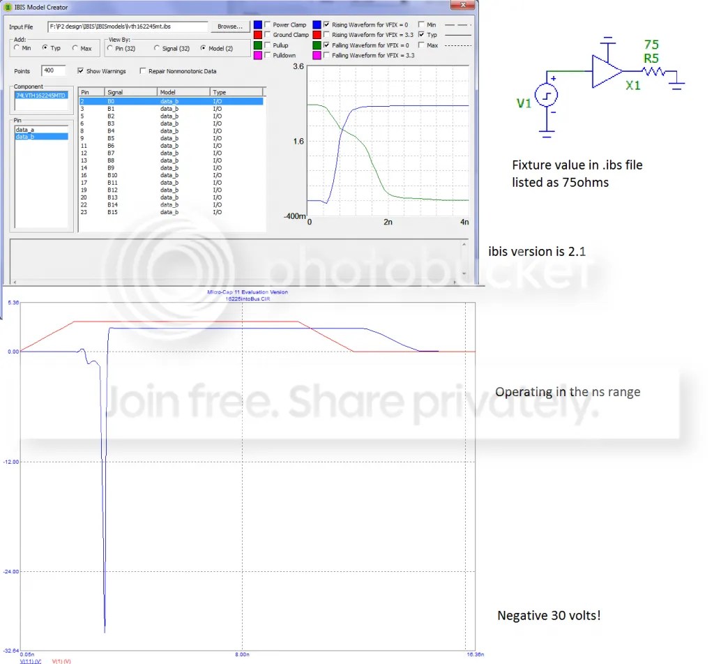
The IC that I am using is a buffer with ns rise time. I obtained the file from Fairchild here:
http://www.fairchildsemi.com/pf/74/74LVTH162245.html
I have seen similar problems when trying to model other buffers. Do you have any advice? Is Micro Cap unsuitable for my application?
Thank you for any help.
James M.
May 28, 2014 at 1:59 pm
James, Thank you for your comment. Unfortunately I am not familiar with this model to offer any advice. The part is apparently obsolete, when I open the link. It does specify it as a tri-state buffer with 25 ohm series output resistor. I suggest you contact Fairchild for model support.
Bert Simonovich
May 28, 2014 at 3:02 pm
Hi Everybody,
Is the driver impedance of the IC and the Characteristic impedance of board trace is having relation between them?
Suppose we have IMX6 IC which is having 34 ohm,40 ohm & 60 ohm driver impedance option and for our board we have
to maintain 50 ohn characteristic impedance for single ended lines ? which one of the Driver impedance of IC will be more
suitable for simulation.
Does these Driver impedance of IC and trace characteristic impedance holds any relation?
do we have to do like that Driver impedance of IC + Series Resistor = Trace characteristic impedance?
Kindly guide me.
Thanks & regards
Sandeep Kumar
July 22, 2014 at 2:21 am
Sandeep, I think if you reread the article from the beginning, you will find your answer.
Bert Simonovich
July 22, 2014 at 10:58 am
Hi thanks for the tutorial…..
I have took one DDR2 buffer and done the similar analysis……….i have dew doubts.
1 . the voltage source at the input is pulse source, whether it’s ON and OFF times will have any effect on results.
2. 10ns time you have taken is specific or we can take any time…..i have took 2.01ns, my model has only values upto 2.97ns
“Vp_rise is equivalent to the maximum voltage of Rising Waveform table found in the IBIS model. Vp_fall is equivalent to the minimum voltage of Falling Waveform table.”
these things are not matching with the results in my ibis model.
here are the plots
I don’t know how to insert plot into it…..
here is the link
Kopanati Mallikarjun
September 6, 2014 at 8:14 pm
Hi,
I wonder why people call the drive output impedance as Drive strength in DDR application.
Drive strength will show signal strong or weak; drive output impedance looks for termination purpose.
Maybe the circuit design makes these two parameters have same value?
Thanks
xin
May 26, 2017 at 12:37 pm
[…] Driver’s Output Impedance From IBIS […]
SPI lines calculating the reflected voltage | Inside a Poustinia.
January 8, 2021 at 1:18 am
Hi Mr. Simonovich,
Thanks for this tutorial its pretty good, but I’m looking for your help to clarify the following questions I’ve:
1) How far my points(markers) should be between eachother and the X-distance should be asymetrical?, if is
yes, how much?.
2) What’s the process to take select the to markes where’ we’re going to take as a reference for the Voltage
and current, I mean we can take it whatever we want, right? and if we do that as a consequence we’re
going to have a different termination resistance for each reference points, but in this case what’s the best
approach you could recommed?.
4) Which marker/point would you select as a V1, and V2 on the graph I’ve included.
5) Should I swap my V1 and V2 between eachother because due to the incorrect criterion to select them?.
3) As you can see, I’ve selected/placed my two markers almost from where the curves start to being not
so linear(almost where the knee starts for both sides[on the positive and negative plane], and I did this
in order to have the best symetric excursion on the output pin (please consider I’m using 3.3V as main
power). But I’m not sure If this is the right way to select my two markes/points to be used to calculate
the series resistor for the transmission line or not. Did I missed something, is the approach I’m following
not correct?.
Thank you Mr. Simonovich.
romano088
October 24, 2021 at 4:57 pm
Check this presentation using VI curves. https://ibis.org/summits/jun05/westerhoff.pdf
Bert Simonovich
October 25, 2021 at 8:08 am