Archive for 2020
Single-ended to Mixed-Mode Conversions
Originally published in Signal Integrity Journal Magazine, July 2020
Signal Integrity (SI) engineers almost always have to work with S-parameters. If you haven’t had to work with them yet, then chances are you will sometime in your SI career. As speed moves up in the double-digit GB/s regime, many industry standards are moving to serial link-based architectures and are using frequency domain compliance limits based on S-parameter measurements.
A vector network analyzer (VNA) is the test instrument of choice to measure S-parameters from a device under test (DUT). By definition, each S-parameter (Sij) is the ratio of the sine wave voltage coming out of a port to the sine wave voltage that was going in to a port (Equation 1). Each S-parameter is complex with a magnitude and a phase.

Suffice it to say, for mathematical reasons, the indexes refer to the port in which the voltages are coming or going. This is counter intuitive to our normal train of thought and is important to be cognisant of this relationship when working with S-parameters.
Single-ended S-parameters
Figure 1 shows an example of a 1-Port, 2-Port and 4-Port DUTs and their respective S-parameter matrices representing uniform transmission lines with respective port index labelling. Each S-parameter in the matrix are single-ended measurements from one port to another.
A 1-Port DUT has one S-parameter (S11) shown in red. It is the ratio of the voltage coming out of Port 1 to the voltage going into Port 1. As a measure of reflected energy out of Port 1, it is also known as return loss (RL)
A 2-Port DUT has 4 S-parameters shown in blue. S-parameters with the same index subscript numbers, i.e. S11, S22 are RL. S-parameters with alternate index subscript numbers, are a measure of transmitted energy and is the ratio of the voltage coming out of a Port to the voltage going into the opposite Port. It is also known as insertion loss (IL). For example, S12 is the ratio of the voltage coming out of Port 1 to the voltage going into Port 2, whereas S21 is the ratio of the voltage coming out of Port 2 to the voltage going into Port 1.

Figure 1 From left to right examples of 1-Port (Red), 2-Port (Blue), 4-Port (Black) DUTs and their respective S-parameter matrices.
A 4-Port DUT has 16 S-parameters, divided into 4 quadrants, shown in black. As you can see the number of S-parameter combinations is the square of the number of ports. In this example, the top left quadrant 1 and bottom right quadrant 4 are the same as individual 2-Port DUTs with different port indices. They are described as:
Quadrant 1:
-
S11 is the ratio of the voltage coming out of Port 1 to the voltage going into Port 1. It is the RL out of Port 1.
-
S12 is the IL and is the ratio of the voltage coming out of Port 1 to the voltage going into Port 2. It is the IL from Port 2 to Port 1.
-
S21 is the ratio of the voltage coming out of Port 2 to the voltage going into Port 1. It is the IL from Port 1 to Port 2. For a uniform transmission line, S21 = S12.
-
S22 is the ratio of the voltage coming out of Port 2 to the voltage going into Port 2. It is the RL out of Port 2. For a uniform transmission line, S22 = S11.
Quadrant 4:
-
S33 is the ratio of the voltage coming out of Port 3 to the voltage going into Port 3. It is the RL out of Port 3
-
S34 is the ratio of the voltage coming out of Port 3 to the voltage going into Port 4. It is the IL from Port 4 to Port 3
-
S43 is the ratio of the voltage coming out of Port 4 to the voltage going into Port 3. It is the IL from Port 3 to Port 4. For a uniform transmission line, S43 = S34.
-
S44 is the ratio of the voltage coming out of Port 4 to the voltage going into Port 4. It is the RL out of Port 4. For a uniform transmission line, S44 = S33
S-parameters in the top right quadrant 2 and bottom left quadrant 3 describe the near-end and far-end coupling of the respective ports. When unwanted coupling happens at the near-end, it is referred to as near-end cross talk, or NEXT. When it happens at the far-end, it is known as far-end crosstalk, or FEXT.
Quadrant 2:
-
S13 is the ratio of the voltage coming out of Port 1 to the voltage going into Port 3. It is the coupling or NEXT from Port 3 to Port 1.
-
S14 is the ratio of the voltage coming out of Port 1 to the voltage going into Port 4. It is coupling or FEXT from Port 4 to Port 1.
-
S23 is the ratio of the voltage coming out of Port 2 to the voltage going into Port 3. It is coupling or FEXT from Port 3 to Port 2.
-
S24 is the ratio of the voltage coming out of Port 2 to the voltage going into Port 4. It is coupling or NEXT from Port 4 to Port 2.
Quadrant 3:
-
S31 is the ratio of the voltage coming out of Port 3 to the voltage going into Port 1. It is the coupling or NEXT from Port 1 to Port 3.
-
S32 is the ratio of the voltage coming out of Port 3 to the voltage going into Port 2. It is coupling or FEXT from Port 2 to Port 3.
-
S41 is the ratio of the voltage coming out of Port 4 to the voltage going into Port 1. It is coupling or FEXT from Port 1 to Port 4.
-
S42 is the ratio of the voltage coming out of Port 4 to the voltage going into Port 2. It is coupling or NEXT from Port 2 to Port 4.
Although there is no industry standard for labeling a 4 or more port DUT, a practical way is to use the port order shown so that the 2-Port DUT is a subset of the top left quadrant of the 4-Port DUT. When you do this, the port order labeling is consistent as you increase the number of ports; with odd ports on the left and even ports on the right. S12 and S21 always describe the IL terms; while S13 and S31 define the NEXT terms.
But sometimes 3rd party 4-port S-parameters are labeled with ports 1 and 2 are on the left side, while ports 3 and 4 are on the right side. In this configuration, S31 and S42 are now the IL terms. This is counter intuitive when moving from 2-Port to 4 or more Port DUT and leading to potential confusion when cascading S-parameters to build a channel model, or converting to mixed-mode S-parameters. Whenever you get S-parameter files from 3rd party, it is always prudent to test it and compare IL plots against port order to ensure you are using them correctly.
Typically, 4-port S-parameters are saved in Touchstone format with a .snp extension, where n is the number of ports. Many Electronic Design Automation (EDA) and circuit simulation software tools allows you to view and plot S-parameters from Touchstone files.
Figure 2 is a schematic of a 4-port S-parameter component used in Keysight ADS. When the component is linked to appropriate .s4p touchstone file and ports connected as shown, the 16-port S-parameter matrix can be plotted and analyzed.

Figure 2 Keysight ADS schematic used to plot 4-Port single-ended S-parameters.
The 1-port and 2-port S-parameters are included in the same plot as the 4-port S-parameters plotted in Figure 3. The top left (red) and bottom right (green) quadrants plot the return loss (RL) and insertion loss (IL), while the top right (blue) and bottom left (magenta) quadrants plot the NEXT and FEXT.

Figure 3 An example of 4-Port S-parameter single-ended plots of a uniform transmission line.
Mixed-mode S-parameters
SI engineers often have to check channel models and S-parameter measurements against industry standard compliance plots. Many of those plots are in terms of mixed-mode S-parameters, which means the single-ended measurements need to be converted to mixed-mode matrix.
Two single-ended transmission lines with coupling are also known as a differential pair, as shown in Figure 4. When we talk about single-ended transmission lines with coupling, we are usually interested in their single-ended properties like characteristic impedance (Zo), phase delay, and NEXT/FEXT relationships as described above.
But when we talk about a differential pair, we are interested in the mixed-mode S-parameters like differential and common signals and how they interact within the pair. Because we are describing the exact same interconnect, they are equivalent.
When describing a differential pair, there are only four possible outcomes in response to an input signal as defined by the mixed-mode S-parameter matrix:
-
A differential signal enters the differential pair and a differential signal comes out
-
A differential signal enters the differential pair and a common signal comes out
-
A common signal enters the differential pair and a differential signal comes out
-
A common signal enters the differential pair and a common signal comes out

Figure 4 Single-ended vs mixed-mode S-parameter matrices of two coupled transmission lines.
Mixed-mode S-parameters in each quadrant are described as:
SDD Quadrant (Red):
-
SDD11 is the ratio of the differential signal coming out of Port 1 to the differential signal going into Port 1. It is the differential RL out of Port 1.
-
SDD12 is the ratio of the differential signal coming out of Port 1 to the differential signal going into Port 2. It is the differential IL from Port 2 to Port 1.
-
SDD21 is the ratio of the differential signal coming out of Port 2 to the differential signal going into Port 1. It is the differential IL from Port 1 to Port 2.
-
SDD22 is the ratio of the differential signal coming out of Port 2 to the differential signal going into Port 2. It is the differential RL out of Port 2.
SDC Quadrant (Blue):
-
SDC11 is the ratio of the differential signal coming out of Port 1 to the common signal going into Port 1.
-
SDC12 is the ratio of the differential signal coming out of Port 1 to the common signal going into Port 2.
-
SDC21 is the ratio of the differential signal coming out of Port 2 to the common signal going into Port 1.
-
SDC22 is the ratio of the differential signal coming out of Port 2 to the common signal going into Port 2.
SCD Quadrant (Magenta):
-
SCD11 is the ratio of the common signal coming out of Port 1 to the differential signal going into Port 1.
-
SCD12 is the ratio of the common signal coming out of Port 1 to the differential signal going into Port 2.
-
SCD21 is the ratio of the common signal coming out of Port 2 to the differential signal going into Port 1.
-
SCD22 is the ratio of the common signal coming out of Port 2 to the differential signal going into Port 2.
SCC Quadrant (Green):
-
SCC11 is the ratio of the common signal coming out of Port 1 to the common signal going into Port 1.
-
SCC12 is the ratio of the common signal coming out of Port 1 to the common signal going into Port 2.
-
SCC21 is the ratio of the common signal coming out of Port 2 to the common signal going into Port 1.
-
SCC22 is the ratio of the common signal coming out of Port 2 to the common signal going into Port 2.
Single-ended S-parameters, with port order shown in Figure 4, can be mathematically converted into mixed-mode S-parameters using equations shown in Table 1.

Alternatively, Keysight ADS can simplify this process using equations on 4-Port single-ended or using 4-port Balun components, as shown in Figure 5.

Figure 5 Keysight ADS schematic used to convert from 4-Port single-ended to 2-Port mixed-mode S-parameters using equations or 4-Port Balun components. Differential and common port numbering as D1, D2, C1, C2 respectively.
Figure 6 plots mixed-mode S-parameters from equations in Table 1. Each quadrant is color coded to coincide with the respective table quadrants.

Figure 6 An example of 4-Port S-parameter mixed-mode plots of a differential transmission line.
References:
[1] M. Resso, E. Bogatin, “Signal Integrity Characterization Techniques”, International Engineering Consortium, 300 West Adams Street, Suite 1210, Chicago, Illinois 60606-5114, USA, ISBN: 978-1-931695-93-0
https://www.amazon.com/Signal-Integrity-Characterization-Techniques-Bogatin-ebook/dp/B07P9277WY/ref=sr_1_fkmr0_1?keywords=bogaitn+resso&qid=1581289220&sr=8-1-fkmr0
[2] A. Huynh, M. Karlsson, S. Gong (2010). Mixed-Mode S-Parameters and Conversion Techniques, Advanced Microwave Circuits and Systems, Vitaliy Zhurbenko (Ed.), ISBN: 978-953-307-087-2,InTech, Available from: http://www.intechopen.com/books/advanced-microwave-circuits-and-systems/mixed-mode-s-parameters-and-conversion-techniques.
[3] Alfred P. Neves, Mike Resso, and Chun-Ting Wang Lee, “S-parameters: Signal Integrity Analysis in the Blink of an Eye”, Signal Integrity Journal, https://www.signalintegrityjournal.com/articles/432-s-parameters-signal-integrity-analysis-in-the-blink-of-an-eye
Keysight Advanced Design System (ADS) [computer software], (Version 2020). URL: http://www.keysight.com/en/pc-1297113/advanced-design-system-ads?cc=US&lc=eng.
Differential Impedance and Why We Care
Originally published in Signal Integrity Journal April 14,2020
What is Differential Impedance and Why do We Care?
Simply put, differential impedance is the instantaneous impedance of a pair of transmission lines when two complimentary signals are transmitted with opposite polarity. For a printed circuit board (PCB) this is a pair of traces, also known as a differential pair. We care about maintaining the same differential impedance for the same reason we care about maintaining the same instantaneous impedance of a single-ended (SE) transmission line: to avoid reflections.
There is really nothing special about differential pairs, other than maintaining the correct differential impedance. But you must understand the implications of the spacing between the traces in a pair.
The differential impedance is simply twice the odd-mode impedance of each trace. SE impedance is the impedance of a single trace and only equals the odd-mode impedance when there is little or no intra-pair coupling between them. When the traces are brought closer together, the differential impedance is reduced, unless the line widths are adjusted to compensate. (More about this later.)
Figure 1 shows the effect on intra-pair coupling of a pair of edge-coupled stripline traces driven differentially. The top figure shows electromagnetic fields surrounding a loosely coupled pair of traces 3.5 line-widths apart. The bottom figure shows a closely coupled pair at 1.5 line-widths apart. The red plus trace is current flowing into the page while the minus blue trace is current flowing out of the page.
The circular lines surrounding each trace are the magnetic fields representing loop inductance. The direction of rotation is based on current direction, using the right-hand rule. The electric field (e-field) lines are perpendicular to the magnetic field lines. They are a measure of capacitance.
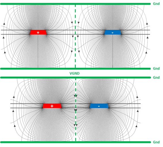
Figure 1. Effect on intra-pair coupling of a pair of edge-coupled stripline traces driven differentially. Top figure shows electromagnetic fields surrounding a loosely coupled pair of traces 3.5 line-widths apart. Bottom figure shows a closely coupled pair at 1.5 line-widths apart.
When the traces are loosely coupled, the electric and magnetic field lines are fairly symmetrical around each trace, and are mirror images of one another about the center line between them. Most of the respective e-field coupling is to the reference ground planes. As the traces are moved closer to one another, the counter-rotating rings compress about the centerline, lowering the inductance. At the same time, more of the e-field lines along the inside edge of each trace tend to couple to one another, increasing the capacitance.
Because of the way the EM-fields interact along the centerline, we can think of it as a virtual ground (VGND) reference plane. They behave exactly the same way as if there is a solid reference plane between them.
Odd-Mode Impedance
Consider a pair of equal width microstrip line traces, labeled 1 and 2, with a constant spacing between them as shown in Figure 2. Assuming lossless transmission lines, each individual trace, when driven in isolation, will have a SE characteristic impedance Zo, defined by the self-loop inductance (L11, L22) and self-capacitance (C11, C22) with respect to the GND reference plane.
When the pair of traces are driven differentially, the mode of propagation is odd. The electromagnetic field interaction is shown in Figure 1. When the intra-pair spacing is close, there will be electromagnetic coupling defined by the mutual inductance (Lm) and mutual capacitance (Cm).
The proximity of the traces to a reference plane influences the amount of electromagnetic coupling between traces. The closer the traces are to the reference plane, the lower the self-loop inductance and stronger self-capacitance; resulting in a lower mutual inductance, and weaker mutual capacitance between traces. The end result is a lower differential impedance.
Figure 2. Pair of microstrip traces showing self-loop inductance (L11, L22), self-capacitance (C11, C22), mutual capacitance (Cm) and mutual inductance (Lm) when line 1 and line 2 are driven differentially.
A 2D field solver is usually used to extract the parameters for a given geometry. Once the resistance, inductance, conductance, and capacitance (RLGC) parameters are extracted, an L C matrix can be set up as follows:
L11 L12 C11 C12
L21 L22 C21 C22
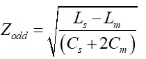
The self-loop inductance and self-capacitance for trace 1 and 2 are L11, C11, L22, C22 respectively. In a perfectly symmetrical differential pair, the off-diagonal (12, 21) terms in each matrix are the mutual inductance and mutual capacitance respectively. The LC matrix can be used to determine the odd-mode impedance. It can be calculated by the following equation [1]:
Equation 1
Where:
Zodd = odd mode impedance
Ls = self-loop inductance = L11 = L22
Cs = self-capacitance = C11 = C22
Lm = mutual inductance = L12 = L21
Cm = mutual capacitance = |C12 |=|C21|
Example
A Polar SI9000 field solver is used to compare a loosely coupled pair, with 4 mil traces, separated by 20 mil space, vs. a SE transmission line with the same dielectric thickness (see Figure 3). The LC matrix was extracted at 10GHz. As can be seen, the odd-mode impedance of the loosely coupled pair equals the characteristic impedance of the SE trace, and thus differential impedance would be the same.
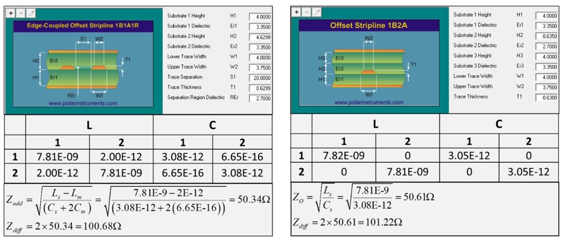
Figure 3. Comparison of a loosely coupled pair (left), with 4 mil traces, separated by 20 mil space, vs. a SE transmission line (right) with the same dielectric thickness. Odd-mode impedance of the loosely coupled pair equals the characteristic impedance of the SE trace.
But if you route a pair of traces with close coupling, the odd-mode impedance is less than the SE impedance for the same trace width (unless you adjust the line width). For example, on the left side of Figure 4, a 4-4-4 mil geometry has a differential impedance of 91 Ohms. In order to get 100 Ohms differential, the line width must be reduced to 3.35 mils and space adjusted to 4.65 mils to keep the same 12 mil center-center pitch, shown on right.

Figure 4. Comparison of 4-4-4 mil geometry (left) vs. 3.35-4.65-3.35 geometry (right) to achieve 100 Ohm differential impedance for the same center-center pitch.
But it doesn’t end there.
For some industry standards, there is usually a very short reach (VSR) spec which has a maximum channel loss defined. For example, the IEEE 802.3 CAUI-4 chip-module (C2M) spec budgets 7.5 dB at 12.89 GHz Nyquist frequency from the chip’s pins to a faceplate module’s pins, e.g. small form-factor pluggable (SFP) module. Because of modern top-of-rack routers and switches, it is not unusual to have 10 or more inches between the main switch chip and SFP module, the differential pair geometry design becomes important to satisfy both differential impedance and insertion loss (IL).
Reduced line width and tighter coupling results in higher loss over the length of the channel. Using the above examples, differential IL is plotted in Figure 5 for all three differential pairs. Loose coupling is shown in green; tight coupling without line width adjustment (Tight1) is shown in red, while tight coupling with line width adjustment (Tight2) is shown in blue.
As you can see, there is about a half dB difference at 12.89 GHz between loose coupling and both tight coupling examples over 10.6 inches. Tight coupling increases IL, regardless if line width is adjusted to meet differential impedance. In this example, there is only 0.1 dB delta between Tight1 and Tight2, which suggests most of the higher loss is due to tighter coupling.
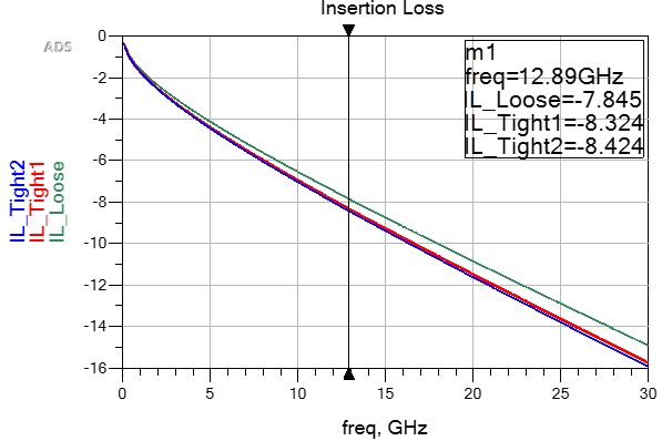
Figure 5. Differential IL comparison of loose coupling (green); Tight1 coupling without line width adjustments (red) and Tight2 coupling with line width adjustment (blue).
This can be explained by reviewing SE to differential mixed-mode conversion. Given a 4-port S-parameter, with SE port order as shown in Figure 6, the differential IL is determined by;
Equation 2
![]()
Where:
SDD21 = the differential IL defined by the ratio of the differential signaling coming out of port 2 to the differential signal going into port 1
S21 = the SE IL defined by the ratio of the SE signaling coming out of port 2 to the SE signal going into port 1
S43 = the SE IL defined by the ratio of the SE signaling coming out of port 4 to the SE signal going into port 3
S23 = far-end crosstalk coupling from port 3 to port 2
S41 = far-end crosstalk coupling from port 1 to port 4
As you can see from Equation 2, when the traces get closer together, and the coupling terms get larger, differential IL increases.
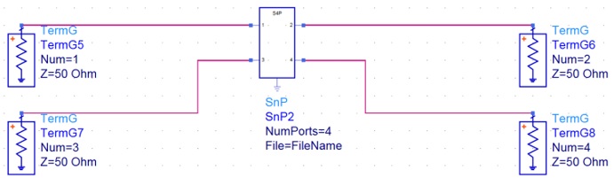
Figure 6. SE 4-port S-parameter port labeling.
Figure 7 plots differential TDR of all three examples. The steeper monotonic rise of the blue trace is due to higher resistive loss of 3.35 mil traces, as compared to the 4 mil traces in the other two examples.
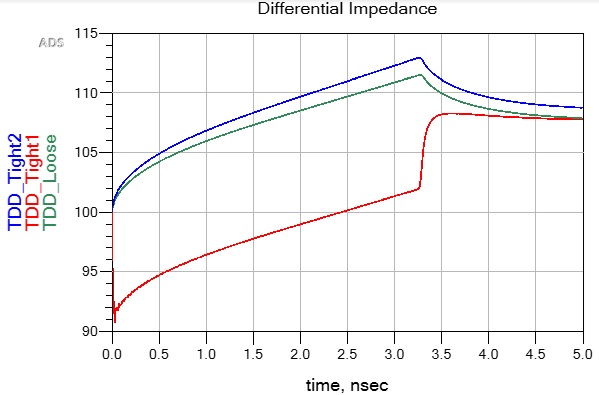
Figure 7. Differential TDR comparison of loose coupling (green); Tight1 coupling without line width adjustments (red) and Tight2 coupling with line width adjustment (blue).
To summarize then, it doesn’t matter if a differential pair is tightly coupled or loosely coupled. Properly engineered, both can be designed to properly match the output driver impedance. But as we have seen, each will have advantages and disadvantages.
Tighter coupling gives you better routing density at the expense of higher loss. Loose coupling allows for easier routing around obstacles and less loss. But in either case, they must be designed and measured for differential impedance.
So why is this important?
PCB fabrication shops use impedance as a metric to determine if the board has been fabricated to specification. Because the odd-mode impedance of a tightly spaced pair of traces depends on driving both traces differentially, you will not be able to determine the differential impedance by just measuring SE impedance of a tightly coupled pair like you could with two uncoupled traces.
References:
-
E. Bogatin, “Signal Integrity Simplified”, 3rd edition, Prentice Hall PTR, 2018
-
Keysight Advanced Design System (ADS) [computer software], (Version 2020)
-
Polar Instruments Si9000e [computer software] Version 2017
How Authorship Advances Your Career and Become an Industry Influencer
 So how can authorship advance your career and lead to becoming an industry influencer?
Well first of all, it offers a chance for deep learning of a subject matter. When you have to capture your thoughts on paper, you suddenly realize you may not know as much about the subject as you think you know. It forces you to do more research on the topic so that the information you are trying to covey is accurate.
It demonstrates thought leadership at your work and the industry. You become the subject matter expert on that topic. And over time, the path to your desk, is worn from all the traffic to your cubicle. If you are self employed as a consultant, it eventually leads to more business opportunities.
It inspires your coworkers and peers to become subject matter experts in their own right by leading by example. Being a subject matter expert offers opportunities to work with other subject matter experts in your company on leading edge projects.
It builds your personal brand. By writing papers and presenting at conferences you become known in the industry from the work you have accomplished and shared.
It gives you a chance to network, meet and collaborate with new people with like interests in the industry. It’s a snowball effect. I can’t even begin to count now many new people from around the world I have met since starting to publish and attend conferences.
It builds self confidence. Everyone at one time or another has had a fear of public speaking. By presenting your work in an audience of your peers, that fear of public speaking begins to dissipate.
Personal pride. Just like a “runner’s high”, you get a dopamine hit every time you see your work published or you present. There is no greater feeling, after spending an enormous amount of time writing your paper, making your slides perfect, continually practicing your presentation, to anyone who will listen, then finally delivering to an audience. It becomes addictive so you will want to continually publish and present your work.
It leaves a lasting legacy of part of your life’s work behind. Let’s face it, our time is limited on this earth. By publishing your work, it inspires future generations in their research, just like past generations of authors have inspired many of today’s authors, including myself.
You don’t have to start big. A personal blog, web site is a good place to begin. Trade journals, and online magazines in your industry are always looking for quality content that is relevant to their readers.
Formal societies, like IEEE, is a more recognized venue and is peer reviewed. Submitting a paper to industry conferences is another way and offers the opportunity to present your work. And finally, the ultimate, is publishing a book.
Once your work is published, then you need to self promote what you have done. Use social media like LinkedIn, Facebook, Twitter or any other platform. You eventually will build a following, who will react and share your posts and soon become an industry influencer.
Finally, I’d like to leave you with this final thought. Being Canadian, our national pastime is Hockey. We usually have a hockey analogy for almost anything. Everyone who follows hockey knows Wayne Gretzky, the greatest hockey player of all time. One of his famous quotes was, “You always miss 100% of the shots you don’t take.” And likewise, if you do not take the shot of writing a paper, book or an article, you cannot become a subject matter expert or industry influencer.
Go for it!
