The Effects on Transmission Line Losses Due to Mixed Reference Plane Roughness Case Study
This article is an edited version of White Paper, “Heuristic Modeling of Transmission Lines due to Mixed Reference Plane Foil Roughness in Printed Circuit Board Stackups” [1].
Designing the right printed circuit board (PCB) stackup can make or break your product performance. If your product has circuitry that is transmission loss sensitive, then paying attention to conductor surface roughness is paramount.
Conductor surface roughness traditionally has been applied to copper foil to promote adhesion to the dielectric material. Early PCBs were only constructed with single or double-sided copper core laminates. The only important metric for copper was its purity and the roughness to improve peel strength. There was no such thing as a PCB stackup and nobody worried about impedance or transmission line losses.
But over the years PCBs have evolved into multi-layer constructions with evermore attention being paid to impedance control and transmission line losses. Thus a PCB stackup definition became vital for consistent performance.
Like any construction project, you need a blueprint before you start building. Similarly for PCBs, you need a stackup drawing and detailed fabrication notes. Part of the stackup design process includes signal integrity (SI) modeling for characteristic impedance and transmission loss. If your design is running at 56Gig pulse amplitude modulation level 4 (PAM-4), for example, you are probably looking at low loss dielectrics and low roughness copper for the signal traces.
But what is sometimes overlooked in the stackup, is the roughness of the reference planes. Often thin core laminate power and ground (GND) planes will specify reverse-treated foils (RTF), which are rougher on the side that bonds to the prepreg. Sometimes one of these planes, usually GND, acts as a reference plane to an adjacent signal layer as shown in Figure 1. If that adjacent high-speed signal layer is using smoother copper than one or both reference planes, a higher insertion loss than expected for that layer will occur and possibly ruin your day.
A similar scenario could occur for high density interconnect (HDI) technology. This is a popular method to increase component density on modern PCBs. By the nature of their stackup construction, a rougher copper reference plane could sometimes also end up adjacent to a signal layer as well. Thus, if insertion loss is a concern, copper foil roughness of reference planes needs to be considered.
Figure 1 An example cross-section stripline geometry from a stackup showing thin core laminate (top) with RTF bonded to prepreg and adjacent to a high-speed differential pair with smooth foil.
So how do you know this before you design your stackup and build your first prototype? Since we do not have any empirical data to go by, we can rely on a heuristic, high-level design (HLD) modeling method starting with published parameters found solely in manufacturer’s data sheets.
Heuristic HLD modeling is a practical technique that is not guaranteed to be perfect, but is still adequate in finding a satisfactory solution sooner, rather than later.
For dielectric parameters, we choose dielectric constant (Dk) / dissipation factor (Df) at or near the Nyquist frequency of the baud rate, then apply effective Dk (Dkeff) correction factor due to roughness, Equation 1 [5].
where:
H = thickness of core/prepreg; Rz is surface roughness of copper; Dk is as published in laminate supplier’s Dk/Df tables. Equation 1 assumes Rz of the foil on each side of the dielectric (core or prepreg) is the same.
For conductor loss, we use Rz roughness numbers from copper suppliers’ data sheets and oxide/oxide alternative Rz roughness numbers from your favorite fab shop, then apply the Cannonball-Huray roughness model [1]-[3].
Cannonball-Huray Model
The original Huray model is defined as:
Equation 2
The Cannonball-Huray model allows you to extract the right parameters using Rz roughness for core and prepreg sides of the foil [1]. Because the Cannonball-Huray model assumes the ratio of Amatte/Aflat = 1, and Ni = 14 spheres, the radius of a sphere (r) can be determined by:
and area of flat tile base (Aflat) by:
Equation 4
Wildriver Isola I-Tera® MT40 Custom Modeling Platform Case Study
To study the effect of reference plane roughness on transmission insertion loss, Wildriver Technology’s [7] custom modeling platform (CMP), shown in Figure 2, was used as a case study. This CMP was custom developed for Isola [6] to characterize their new I-Tera® MT40 very low-loss laminate material.
It combines 27 structures based on a consistent development of primitive structures; useful for performing a host of calibrations including automatic fixture removal, unknown THRU, WinCal XE™ calibration, and VNA gating and time transform analysis.
Figure 2 Wildriver Isola I-Tera® MT40 Custom Modeling Platform. Source: Wildriver Technology [7]
Stackup Validation
The PCB stackup is shown in Figure 3. Often PCB fab shop field application engineers (FAE) modify existing stackups and unintentionally make errors in transferring new parameters from data sheets into their software tools. Also, they may not necessarily know the design intent of the stackup. So the first step for any model correlation exercise is to sanitize the stackup, to ensure it meets the product design intent for signal integrity (SI) performance. In fact that is how the issue of different plane roughness was uncovered.
Since it is always a good practice to ensure the same roughness is specified for reference planes as the adjacent signal layers, I naively assumed it would be the case for any high-speed stackup. But that wasn’t the case here. Layers E1,E2 and E7, E8 specify 1oz RTF, while layers E3, E4 and E5, E6 specify 1oz VLP2 foil. Because the Isola I-Tera® MT40 CMP is intended to aid in modeling test structures, this is not a fatal flaw. On the contrary, it is a perfect platform to assess the effect of rougher reference planes.
Figure 3 Isola I-Tera® MT40 Custom Modeling Platform stackup. Source: Wildriver Technology [7]
Upon further review, it was discovered that the core laminates between E3,E4 and E5, E6 specified 1067/2×3313 glass styles, but this combination was not listed for 12 mil thickness. Instead, only 3×3313 core is offered. Because of that, the Dk shown is also wrong and will affect the impedance of the traces. The right Dk for 3×3313 is 3.53 instead if 3.33.
Foil Roughness
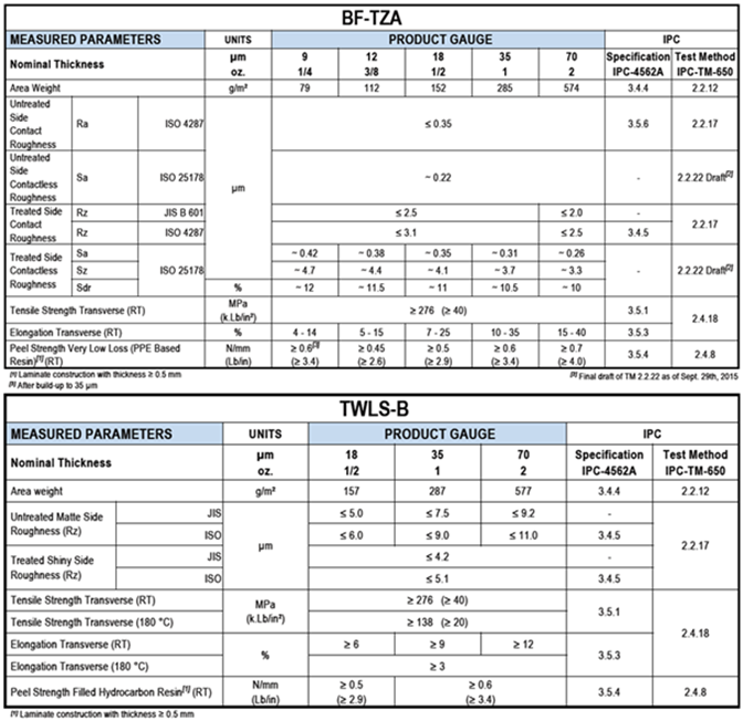
As mentioned earlier, the roughness of the foil affects the effective Dk, so we need to use the right number for our model validation. The standard VLP2 foil, used on I-Tera® MT40 core laminates is BF-TZA foil. Optional RTF foil, used for layers E1, E2 and E7, E8, is TWLS-B. Both are from Circuit Foil [8].
Relevant roughness parameters are shown in Figure 4. For the core side of the foil we are interested in the Rz parameters for the treated side listed in the table. But there are two Rz parameters, JIS B 601 and ISO 4287 specified. So which one do we use for modeling?
From IPC-TM-650 Section 1.2 [11] states, “The foil profile of foils shall be evaluated using the parameter Rz (DIN) or RTM, which is defined as the average maximum peak to valley height of five consecutive sampling lengths within the measurement length. This value is approximately equivalent to the values of profile determined from microsectioning techniques.”
and;
Section 1.3 states, “RZ (ISO) is a different parameter from Rz (DIN) and is not applicable to this method.”
Rz JIS represents the 10-point mean value, which is the sum of the average of the 5 highest peaks and the 5 lowest valleys over the sample length. Rz DIN is similar; except it is defined as the average maximum peak to valley height of five consecutive sampling lengths within the measurement length. Thus we will use Rz JIS for modeling analysis.
Figure 4 Roughness parameters from Circuit Foil [8] data sheets. Top is VLP2 standard foil used on I-Tera® MT40, while bottom is RTF option used for relevant layers in the stackup
Determine Effective Dk Due to Roughness
The first step in HLD impedance modeling is to gather all the dielectric and foil data sheet parameters to determine the effective Dk.
Figure 5 summarizes thickness of core, prepreg and signal trace from the stackup geometry in Figure 3. Note that photos are for illustrative purposes only and are not actual cross-sections from CMP PCB. Dk for core and prepreg were obtained from Isola I-Tera® MT40 Dk/Df tables [6].
Figure 5 Data sheet parameters for RTF/VLP2 foil roughness and dielectric properties for I-Tera® MT40 stackup geometry. Note: Photos are for illustrative purposes only and are not actual cross-sections from CMP PCB. Surface roughness pictures source: Circuit Foil [8]
The top reference plane is TWLS-B RTF foil with matte side 1 ≤ 7.5 JIS, obtained from Circuit Foil data sheet (Figure 4). The roughness surface profile is shown in the upper left. After OA smoothing, 1 ≤ 6.23 [1].
BF-TZA foil is used for both sides of the core laminate. The top surface of the stripline trace, shown in the upper right picture, is the drum side of the foil, before OA treatment. After OA treatment, Rz2 ~ 1.9 μm [1].
The bottom surface profile of the stripline trace and the top surface of the bottom reference plane are the treated matte sides of the foil, shown in the bottom right and bottom left pictures respectively. They both share the same roughness (Rz3, Rz4 =2.5μm JIS) from the BF-TZA data sheet (Figure 4).
The next step is to convert the imperial thickness units to metric, then use Equation 1 to determine Dkeff due to roughness for the prepreg and core.
Determine Cannonball-Huray Roughness Parameters
Several popular electronic design automation (EDA) tools include the Cannonball-Huray model directly as an option, so the respective Rz parameter is all that is needed.
Any of these tools can be used for HLD modeling, but my favorite is Polar SI9000 [9] because of its simplicity and sufficient accuracy for prefabrication modeling and analysis. Many fab shops use this tool for impedance prediction, so it is easy to stay in sync with them during the HLD stage of your project. Plus, it has the added benefit of modeling transmission loss and exporting S-parameters in touchstone format for further channel modeling in other tools.
Because Polar Si9000 assumes all the reference planes have the same roughness, it only allows Rz roughness parameters to be inputted for the matte and drum side of the signal trace. The best we can do, is take the average roughness of Rz1,Rz2 and Rz3,Rz4:
Simulation Correlation
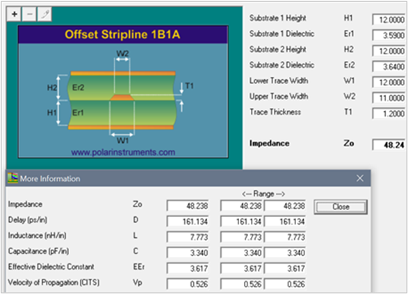
When Dkeff due to roughness values were used instead of published Dk values, the new impedance prediction is 48.24 ohms, as shown in Figure 6.
Figure 6 Polar Si9000 impedance prediction with Dkeff due to roughness
Dkeff/Df for H1, H2 was then inputted into the causal dielectric model at 10GHz, as shown in Figure 7 (left), while Rzmatte, Rzdrum was inputted into the Cannonball-Huray model (right).
Figure 7 Causal Dkeff/Df dielectric and Cannonball-Huray roughness model input panels in Polar Si9000
After a 6-inch transmission line was simulated, the S-parameters were exported in touchstone format. Keysight Pathwave ADS [10] was used for further processing and analysis.
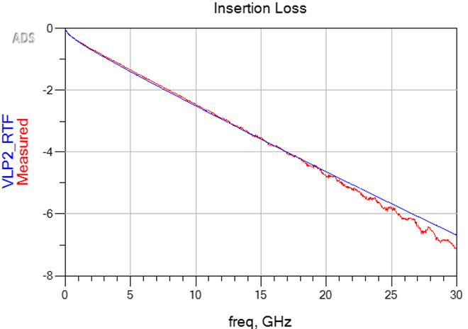
Figure 6 compares simulated insertion loss vs de-embedded reflectionless generalized modal (GM) S-parameter measurements, provided by Wildriver Technology [7]. As you can see there is excellent correlation without fitting to measured data!
Figure 8 HLD Insertion Loss simulation correlation for as designed stackup from data sheet and stackup parameters
Figure 9 plots simulated Dkeff vs measurements. At 10 GHz, simulated Dkeff is 0.105 (-2.8%) lower than measured value. Without actual cross-section microscopic measurements, it is difficult to conclude if the published Dk is wrong, or if there is process variation with roughness parameters used in the model.
But it is also interesting to note that measured Dkeff is not a constant value over frequency, as shown in the I-Tera® MT-40 Dk/Df tables. Instead Figure 9 reveals it varies over frequency, so the Dk/Df data sheet numbers are suspect.
Regardless, for the HLD modeling process, the simulation results are within acceptable tolerance.
Figure 9 HLD Dkeff simulation correlation for as designed stackup
Exploring the Effects of Alternate Foil Roughness
Now that we have good correlation to measurements, we can repeat the HLD modeling process to explore different foil roughness options. Figure 10 summarizes the thickness of core, prepreg and signal trace for VLP2/VLP2 foil (top) and VLP1/VLP1 foil (bottom). Note that photos are for illustrative purposes only and are not actual cross-sections from CMP PCB.
Respective Dkeff, and Cannonball-Huray roughness parameters were recalculated with same steps as VLP2/RTF case above.
Figure 10 Alternate foil options simulated for what-if loss comparison. Top is VLP2/VLP2 foil parameters for all copper layers and bottom is VLP1/VLP1 foil parameters for all copper layers. Note: Photos are for illustrative purposes only and are not actual cross-section from CMP PCB. Surface roughness pictures source: Circuit Foil [8]
Figure 11 presents the simulation results of all three scenarios. As expected. when the reference plane foil roughness went from RTF/VLP2 to VLP2/VLP2 there was improvement. At 14 GHz it was 0.5 dB and at 28GHz it was 1 dB improvement.
When VLP1/VLP1 foil was used, it was further improved by 0.8 dB and 1.7 dB at 14 GHz and 28 GHz respectively. So if your design is loss sensitive, you might want to consider VLP1 foil option.
When we compare Dkeff plots, we see effective Dk approaches actual Dk/Df data sheet values in the tables when smoother copper is used, as expected [5].
Since Dkeff was derived by phase delay, propagation delay will be affected by rougher copper.
Figure 11 What-if simulation comparison of VLP2/RTF, VLP2/VLP2, VLP1/VLP1 foil options and their effect on insertion loss and Dkeff
Conclusions
1. Roughness of reference planes make a significant difference in loss and phase delay, especially if one of the reference planes is RTF. If loss is important then all high-speed reference planes should have the same foil roughness specified
2. Heuristic HLD modeling method is a useful and accurate way to determine prefabrication impedance and loss predictions using data sheet parameters.
3. Published Dk from I-Tera® MT40 Dk/Df data sheet tables is not a flat constant over frequency.
4. Confirmed Rz JIS is the right parameter to use from Circuit Foil data sheet, instead of Rz ISO.
Acknowledgements
· Al Neves, CTO Wildriver Technology, for providing the custom modeling platform design details and measured data for the case study.
· Michael Gay, Director Business Development – Strategic Accounts at Isola Group, for providing foil supplier’s data sheets used on I-Tera® MT40 laminates.
References
[1] B. Simonovich, “Heuristic Modeling of Transmission Lines due to Mixed Reference Plane Foil Roughness in Printed Circuit Board Stackups”, White Paper, Lamsim Enterprises Inc.
[2] B. Simonovich, “Practical Method for Modeling Conductor Surface Roughness Using The Cannonball Stack Principle”, White Paper, Lamsim Enterprises Inc.
[3] L. Simonovich, “Practical method for modeling conductor roughness using cubic close-packing of equal spheres,” 2016 IEEE International Symposium on Electromagnetic Compatibility (EMC), 2016, pp. 917-920, doi: 10.1109/ISEMC.2016.7571773.
[4] L. Simonovich, “PCB Interconnect Modeling Demystified”, DesignCon 2019, Proceedings, Santa Clara, CA, 2019
[5] B. Simonovich, “A Practical Method to Model Effective Permittivity and Phase Delay Due to Conductor Surface Roughness”. DesignCon 2017, Proceedings, Santa Clara, CA, 2017
[6] Isola Group S.a.r.l., 3100 West Ray Road, Suite 301, Chandler, AZ 85226, URL: http://www.isola-group.com/
[7] Wild River Technology LLC 8311SW Charlotte Drive Beaverton, OR 97007, URL: https://wildrivertech.com/
[8] Circuit Foil 6 Salzbaach, 9559 Wiltz, Grand Duchy of Luxembourg URL: https://www.circuitfoil.com/portfolio/
[9] Polar Instruments Si9000e [computer software] Version 2018, URL: https://www.polarinstruments.com/index.html
[10] Keysight Pathwave Advanced Design System (ADS) [computer software], (Version 2021 update2). URL:http://www.keysight.com/en/pc-1297113/advanced-design-system-ads?cc=US&lc=eng.
[11] IPC-TM-650 Test Methods Manual 2.2.17A, Surface Roughness and Profile of Metallic Foils (Contacting Stylus Technique), 2/2001 Rev. A
[12] IPC-TM-650, 2.5.5.5, Rev C, Test Methods Manual


Leave a comment